Light emissive element having pixel sensing circuit

a technology of light emissive elements and sensing circuits, which is applied in the field of sensing a light emissive element in an active matrix display pixel cell, can solve the problems of severe problems, significant size, and inhomogeneity defects or structural inhomogeneities, and achieve the effect of improving the reverse biasing of the light emissive elemen

Active Publication Date: 2008-09-09
INNOLUX CORP
View PDF8 Cites 150 Cited by
  • Summary
  • Abstract
  • Description
  • Claims
  • Application Information

AI Technical Summary

Benefits of technology

[0011]An object with the present invention is to overcome this problem, and to prov...

Problems solved by technology

Defects or structural inhomogeneities, for example particles from the substrates or from the processing of the device and pinholes and hillocks in the layers, are a severe problem for the lifetime of all OLED displays (including polymer and small molecules, segmented, passive matrix and active matrix displays).
Such a ...

Method used


Image

  • Light emissive element having pixel sensing circuit
  • Light emissive element having pixel sensing circuit
  • Light emissive element having pixel sensing circuit

Examples


Embodiment Construction

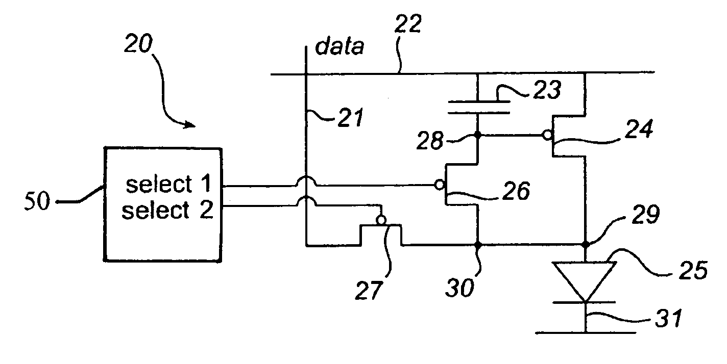
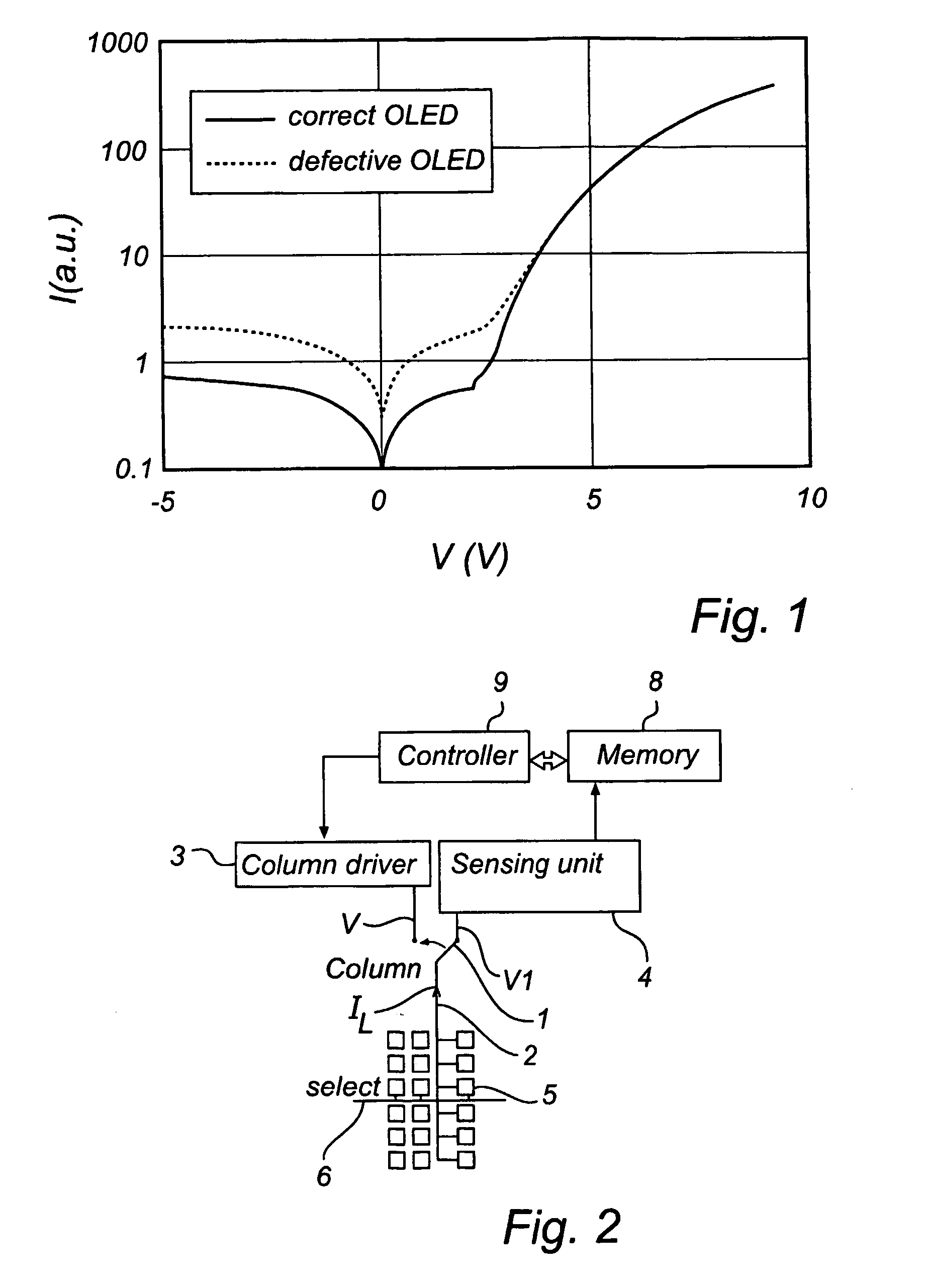
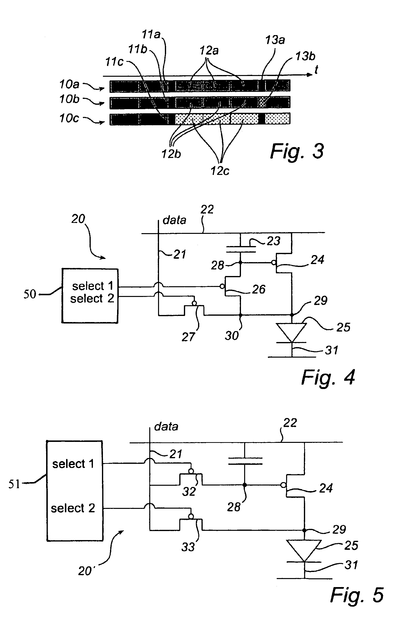
[0031]By means of a switch 1 on the top of the data column line 2 outside the display area, the data column line 2 can be switched between a conventional column driver 3 providing a drive signal, here a voltage (V) but alternatively a current, representing image display data, and a sensing unit 4 providing a negative (with respect to the OLED cathode) sensing voltage (V1). This negative voltage will reverse bias the OLED in the currently addressed pixel cell 5, and enable a leakage current (IL) to flow through the data column line 2.

[0032]The method according to the invention requires a special addressing dividing the time into output periods and sensing periods. During the output periods (or frames) the switch 1 is connected to the column driver 3 and data is programmed into the pixels 5 to light up the OLED. In between these output periods, the switch 1 is connected to the sensing unit 4. The pixels 5 are then unlit and instead leakage currents IL from the OLEDs are detected.

[0033...


PUM


Abstract

A method for sensing a light emissive element in an active matrix display pixel cell further including a data line connectable to a drive element and to a first electrode of the emissive element. The data line is connected to the anode of the emissive element, and a sensing voltage to reverse bias the emissive element, and detecting any leakage current flowing through the emissive element.

Description

BACKGROUND OF THE INVENTION[0001](1) Field of the Invention[0002]The present invention relates to method for sensing a light emissive element in an active matrix display pixel cell. It also relates to an active matrix display, comprising a plurality of pixel cells each having a current driven light emissive element such as an organic or polymer light emitting diode and a data line connectable to a drive element and to an electrode of the emissive element.[0003](2) Description of Related Art[0004]Defects or structural inhomogeneities, for example particles from the substrates or from the processing of the device and pinholes and hillocks in the layers, are a severe problem for the lifetime of all OLED displays (including polymer and small molecules, segmented, passive matrix and active matrix displays).[0005]Initial screening and burn-in procedures can be applied to reduce defects appearing during the manufacturing process, but such defects can also be activated during the lifetime o...

Claims


Application Information

Patent Timeline
IPC IPC(8): G09G3/32G01R31/28G09G3/00G09G3/30
CPCG09G3/006G09G3/3233G09G3/3208G09G2330/10G09G2310/0256G09G2320/0285G09G2320/043G09G2300/0842G09G3/30
Inventor GIRALDO, ANDREAJOHNSON, MARK THOMAS
Owner INNOLUX CORP
Why Eureka
Try Eureka