Gated clock conversion

a clock and gate technology, applied in the field of programmable devices, can solve the problems of affecting the timing of the clock,

Inactive Publication Date: 2008-09-09
ALTERA CORP
View PDF3 Cites 13 Cited by
  • Summary
  • Abstract
  • Description
  • Claims
  • Application Information

AI Technical Summary

Benefits of technology

[0010]In an embodiment, the method reduces the Boolean expression to cofactors of the first input variable and evaluates the cofactors for values of a set of input values of at least the second input variable. In response to a determination that one of the cofactors has a constant value for the set of input values, the embodiment of the method modifies the design by connecting the clock input of the component with the base clock signal and connecting the data input of the component with a modified data signal. The modified data signal is provided by input logic performing a second function of the data signal and a second input signal.

Problems solved by technology

However, some programmable devices have only a limited amount of resources available for global clock networks.
Thus, the large number of clock trees of the ASIC design can overwhelm the resources of the programmable device.
Additionally, even if a programmable device has sufficient resources to implement all of the numerous clock trees of a complex ASIC design, timing closure problems often arise.
Programmable logic cells are relatively slow as compared with dedicated logic circuits.
Because of their relatively slow operating speed, the programmable logic cells implementing gated clock logic introduce substantial clock skew between registers and other components using the base clock signal and those using gated clock signals.
Previously, designers would have to perform this conversion manually, which is not only tedious and time-consuming but also potentially error-prone.

Method used


Image

  • Gated clock conversion
  • Gated clock conversion
  • Gated clock conversion

Examples


Embodiment Construction

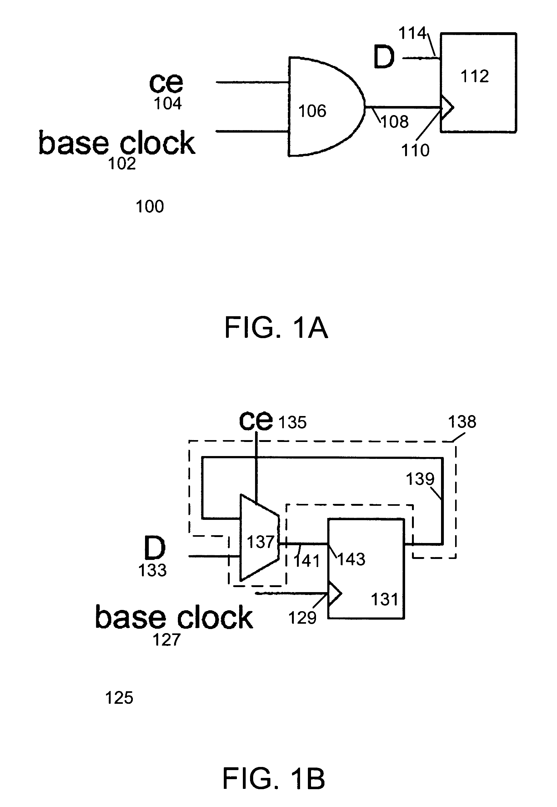
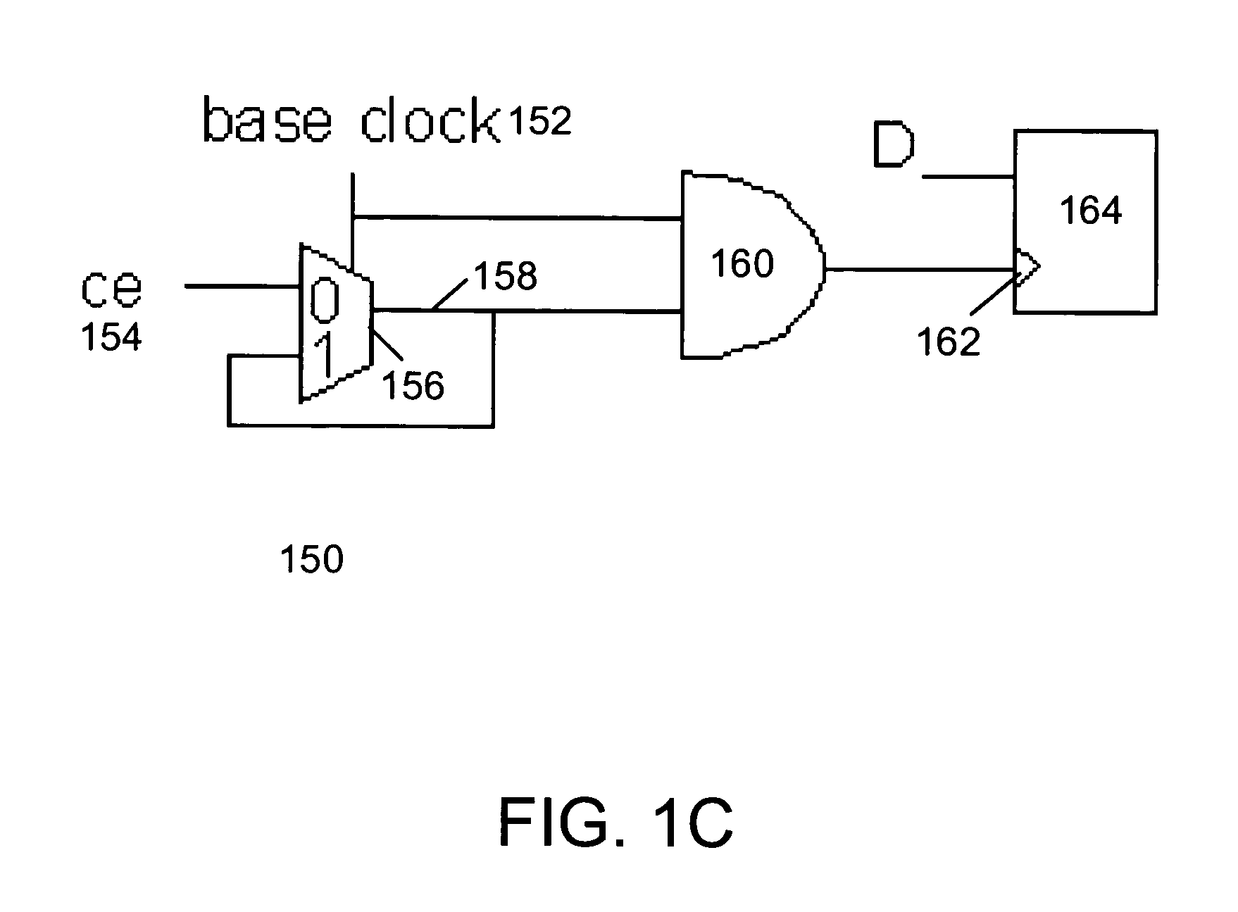
[0020]FIGS. 1A-1C illustrate an example gated clock input and corresponding clock enable input logic suitable for use with an embodiment of the invention. FIG. 1A illustrates an example design 100 including a gated clock signal. Example design 100 includes a base clock signal 102 and a clock enable signal 104 connected with combinatorial logic 106. The output of the combinatorial logic 106 is a gated clock signal output 108. The gated clock signal output 108 is connected with a clock input 110 of a register 112. Register 112 also includes a data input 114.

[0021]In this example 100, the combinatorial logic 106 includes an AND logic gate. Thus, when the clock enable signal 104 is asserted, the base clock signal 102 will pass through the combinatorial logic 106 and produce a corresponding clock signal from gated clock signal output 108. Conversely, when the clock enable signal 104 is deasserted, the gated clock signal output 108 will be constant. As a result, the operation of the regis...


PUM


Abstract

Gated clock signals in ASIC designs are automatically optimized for implementation with a programmable device. Components having gated clock signals are identified and converted to operate directly from the base clock signal. To maintain compatibility, the data signal to the component is modified to connect with additional input logic responsive to a clock enable signal. The input logic modifies the signal received by the component's data input so that the component's output in response to the clock enable signal is unchanged. To this end, a system and method may identify the logic cone associated with a gated clock signal, convert this logic cone into a Boolean expression, and determine cofactors of the base clock signal from this Boolean expression. The input logic and clock enable logic are derived from an analysis of the cofactors of the base clock signal.

Description

BACKGROUND OF THE INVENTION[0001]The present invention relates to the field of programmable devices, and the systems and methods for programming the same. Programmable devices, such as FPGAs, typically includes thousands of programmable logic cells that use combinations of logic gates and / or look-up tables to perform a logic operation. Programmable devices also include a number of functional blocks having specialized logic devices adapted to specific logic operations, such as adders, multiply and accumulate circuits, phase-locked loops, and one or more embedded memory array blocks. The logic cells and functional blocks are interconnected with a configurable switching circuit. The configurable switching circuit selectively routes connections between the logic cells and functional blocks. By configuring the combination of logic cells, functional blocks, and the switching circuit, a programmable device can be adapted to perform virtually any type of information processing function.[000...

Claims


Application Information

Patent Timeline
Patent Type & Authority Patents(United States)
IPC IPC(8): G06F17/50
CPCG06F17/5054G06F2217/62G06F30/34G06F30/396G06F2117/04G06F30/343
Inventor YUAN, JINYONG
Owner ALTERA CORP
Why Eureka
Try Eureka