

Charge pump
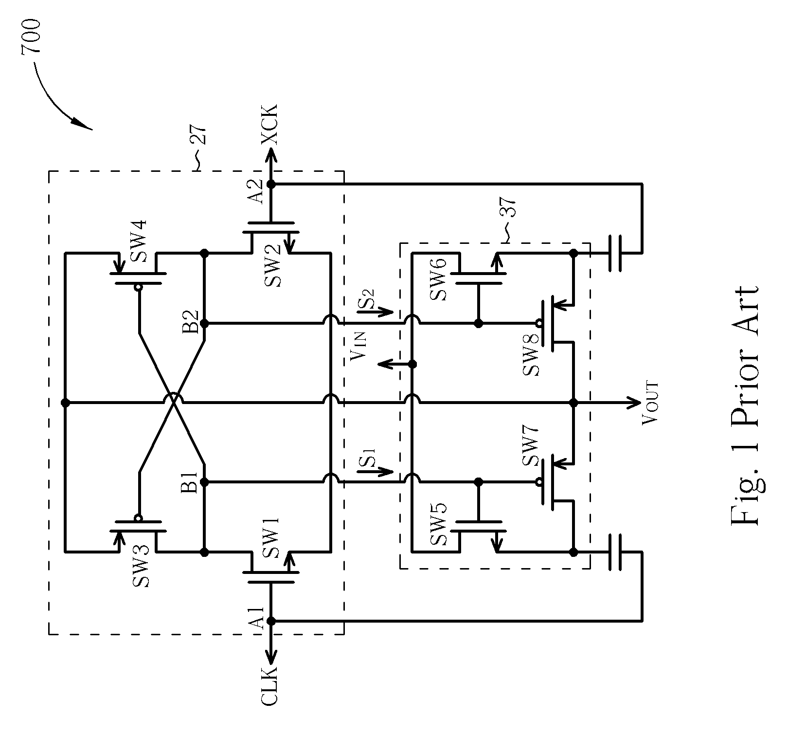
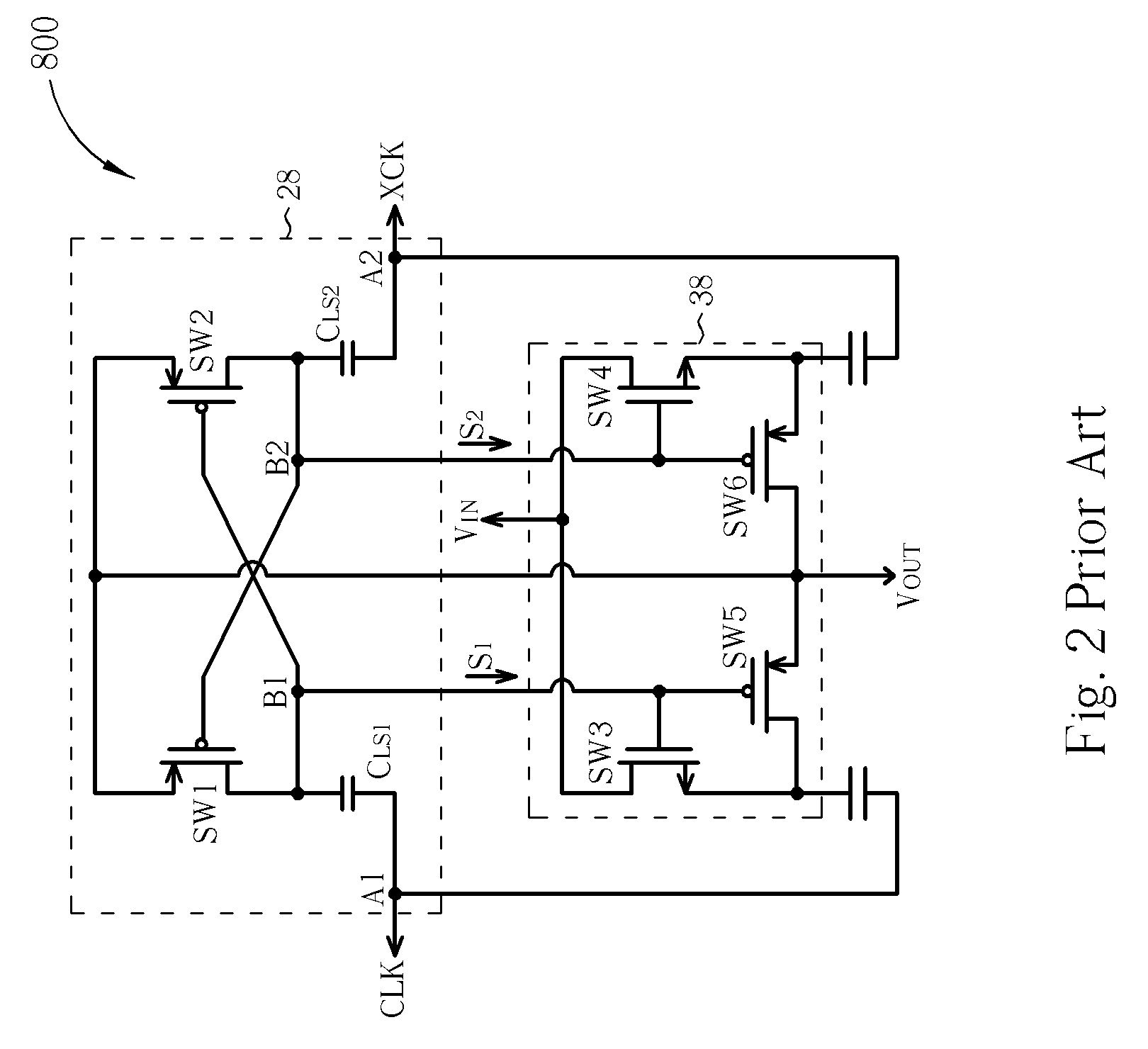
a technology of charge pump and charge pump body, which is applied in the direction of dc-dc conversion, power conversion system, instruments, etc., can solve the problems of less stable output voltage of capacitive push-pull charge pump b>800/b>, easy varies, and inability to provide control signals sb>1, and achieve the effect of enhancing the level of first and second clock signals, and enhancing the level of input voltag
- Summary
- Abstract
- Description
- Claims
- Application Information
AI Technical Summary
Benefits of technology
Problems solved by technology
Method used
Image

Examples
first embodiment
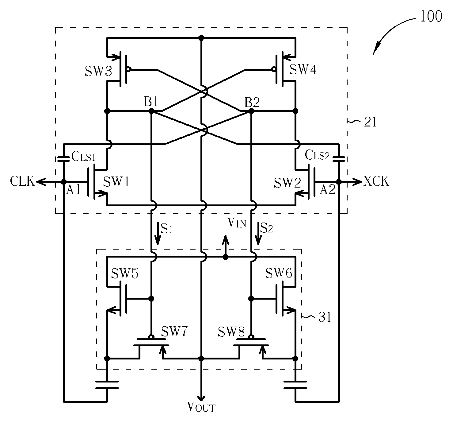
[0021]Reference is made to FIG. 3 for a diagram of a positive-polarity charge pump 100 according to the present invention. The positive-polarity charge pump 100 includes a level shifter circuit 21 and a charge exchange control switching circuit 31. The level shifter circuit 21 includes switches SW1-SW4 and capacitors CLS1 and CLS2. The charge exchange control switching circuit 31 includes switches SW5-SW8. VIN and VOUT represent the voltages established at an input end and an output end of the positive-polarity charge pump 100, respectively. The switches SW1, SW2, SW5 and SW6 can include NMOS transistors, and the switches SW3, SW4, SW7 and SW8 can include PMOS transistors.
[0022]In the level shifter circuit 21, the gates of the switches SW1 and SW2 are respectively coupled to the nodes A1 and A2. The drains of the switches SW1 and SW2 are respectively coupled to the nodes B1 and B2, and the sources of the switches SW1 and SW2 are coupled to each other. The gates of the switches SW3 a...
second embodiment
[0025]Reference is made to FIG. 4 for a diagram of a positive-polarity charge pump 200 according to the present invention. The positive-polarity charge pump 200 includes a level shifter circuit 22 and a charge exchange control switching circuit 32. The level shifter circuit 22 includes switches SW1-SW4 and capacitors CLS1 and CLS2. The charge exchange control switching circuit 32 includes switches SW5-SW10. VIN and VOUT represent the voltages established at an input end and an output end of the positive-polarity charge pump 200, respectively. The switches SW1, SW2, SW5 and SW6 can include NMOS transistors, and the switches SW3, SW4, SW7-SW10 can include PMOS transistors.
[0026]In the level shifter circuit 22, the gates of the switches SW1 and SW2 are respectively coupled to a node A1 and a node A2. The drains of the switches SW1 and SW2 are respectively coupled to a node B1 and a node B2, and the sources of the switches SW1 and SW2 are coupled to each other. The gates of the switches...
third embodiment
[0029]Reference is made to FIG. 5 for a diagram of a negative-polarity charge pump 300 according to the present invention. The negative-polarity charge pump 300 includes a level shifter circuit 23 and a charge exchange control switching circuit 33. The level shifter circuit 23 includes switches SW1-SW4 and capacitors CLS1 and CLS2. The charge exchange control switching circuit 33 includes switches SW5-SW8. VIN and VOUT represent the voltages established at an input end and an output end of the negative-polarity charge pump 300, respectively. The switches SW1 and SW2 can include PMOS transistors, and the switches SW3-SW8 can include NMOS transistors.
[0030]In the level shifter circuit 23, the gates of the switches SW1 and SW2 respectively receive clock signals CLK and XCK. The drains of the switches SW1 and SW2 are respectively coupled to the nodes B1 and B2, and the sources of the switches SW1 and SW2 are coupled to the input end of the negative-polarity charge pump 300. The gates of...
PUM
 Abstract
Description
Claims
Application Information