Booster power management integrated circuit chip with ESD protection between output pads thereof

a technology of power management and integrated circuits, applied in the direction of instruments, pulse techniques, semiconductor/solid-state device details, etc., can solve the problems of instantaneous high voltage discharge having an adverse effect on the electric circuit connected to the terminal, the most common causes of failure in electronic systems, and the concentration of higher electric curren

Inactive Publication Date: 2008-10-14
RICHTEK TECH
View PDF3 Cites 39 Cited by
  • Summary
  • Abstract
  • Description
  • Claims
  • Application Information

AI Technical Summary

Problems solved by technology

In particular, when an object that carries static electricity comes into contact with a terminal of an integrated circuit chip, an instantaneous high voltage discharge can have an adverse affect on electric circuits connected to that terminal.
This phenomenon, which is known as electrostatic discharge (abbreviated as ESD), is one of the most common causes of failure in electronic systems.
However, when the BJT 110 conducts, it has a non-uniform characteristic in that higher temperatures can cause higher electric current concentration.
However, the resistor 46 will affect the output voltage of the booster 4, thereby adversely affecting operating efficiency of the booster 4.
However, in view of circuit size considerations, it is not possible to add a sufficiently large series resistance for the parasitic BJT.
As a result, the MOS transistor switch 41 is prone to burn out due to the heat concentration effect of the electric currents generated during the occurrence of ESD.

Method used


Image

  • Booster power management integrated circuit chip with ESD protection between output pads thereof
  • Booster power management integrated circuit chip with ESD protection between output pads thereof
  • Booster power management integrated circuit chip with ESD protection between output pads thereof

Examples


Embodiment Construction

[0032]Before the present invention is described in greater detail with reference to the accompanying preferred embodiments, it should be noted herein that like elements are denoted by the same reference numerals throughout the disclosure.

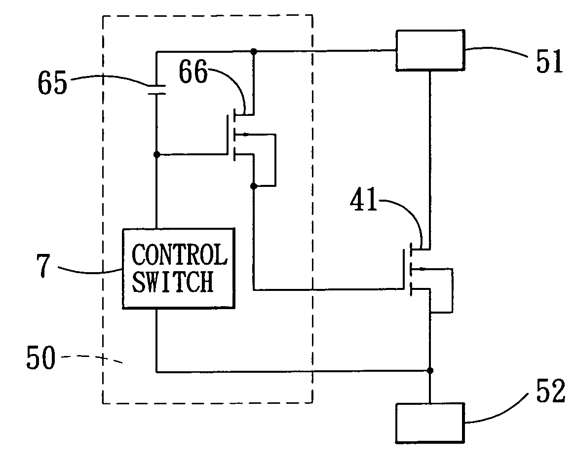
[0033]Referring to FIG. 6, the preferred embodiment of a booster power management integrated circuit chip 6 with an ESD protection mechanism of this invention is applied in a booster (or boost converter) 4. Aside from the components of the conventional power management integrated circuit chip 5 shown in FIG. 4, the power management integrated circuit chip 6 of this invention further includes a trigger circuit 50 coupled between first and second output pads 51, 52, and is further coupled to a gate of MOS transistor switch 41. When an instantaneous voltage (e.g. due to ESD) larger than a trigger voltage level is present between the first and second output pads 51, 52, the trigger circuit 50 will drive the MOS transistor switch 41 to conduct so as to e...


PUM


Abstract

A booster power management integrated circuit chip includes first and second output pads, a transistor switch coupled between the first and second output pads and having a gate, and a trigger circuit coupled between the first and second output pads and further coupled to the gate of the transistor switch. The trigger circuit drives the transistor switch to conduct when an instantaneous voltage larger than a trigger voltage level is present between the first and second output pads so as to enable electric current to flow through the transistor switch.

Description

CROSS-REFERENCE TO RELATED APPLICATION[0001]This application claims priority of Taiwanese application no. 093138396, filed on Dec. 10, 2004.BACKGROUND OF THE INVENTION[0002]1. Field of the Invention[0003]The invention relates to a booster power management integrated chip, more particularly to a booster power management integrated circuit chip that includes an electrostatic discharge (ESD) protection mechanism.[0004]2. Description of the Related Art[0005]Static electricity is always present in our surrounding environment. In particular, when an object that carries static electricity comes into contact with a terminal of an integrated circuit chip, an instantaneous high voltage discharge can have an adverse affect on electric circuits connected to that terminal. This phenomenon, which is known as electrostatic discharge (abbreviated as ESD), is one of the most common causes of failure in electronic systems.[0006]As shown in FIG. 1, a conventional ESD protection circuit 1 is embedded i...

Claims


Application Information

Patent Timeline
Patent Type & Authority Patents(United States)
IPC IPC(8): H02H9/00H01L23/62H02M3/155H03K17/0814H03K17/082
CPCH02M3/155H02M1/32H03K17/08142H03K17/0822
Inventor SU, HUNG-DERLIU, JING-MENGKU, CHIANG-YUNG
Owner RICHTEK TECH
Why Eureka
Try Eureka