Reactor with heated and textured electrodes and surfaces

Inactive Publication Date: 2008-10-21
OEM GRP LLC
View PDF39 Cites 25 Cited by
  • Summary
  • Abstract
  • Description
  • Claims
  • Application Information

AI Technical Summary

Benefits of technology

[0013]It is a further object of the present invention to provide a deposition shield which can be at least one of heated and/or textured in order to ensure that any materials deposited thereon adhere to the surface and do not flake or spauld off, potentially interfering with the processing o

Problems solved by technology

The deposits which form on the various surfaces found in the reactor are known to have a detrimental effect to the fabrication of the semiconductor wafer product in the reactor.
By way of example only, such deposits and layers on surfaces of the reactor can be thick and have poor reactor surface adhesion qualities.
Additionally, the deposits or layers may not be very durable.
All this potentially leads

Method used


Image

  • Reactor with heated and textured electrodes and surfaces
  • Reactor with heated and textured electrodes and surfaces
  • Reactor with heated and textured electrodes and surfaces

Examples


Embodiment Construction

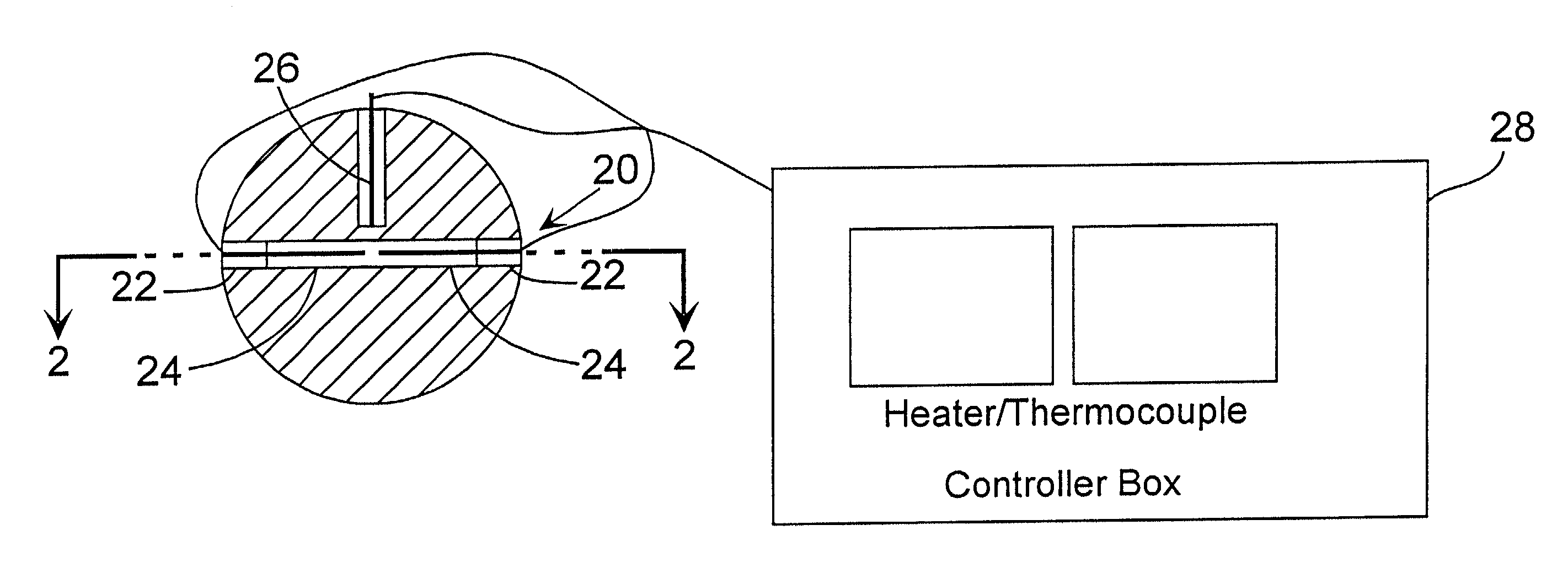
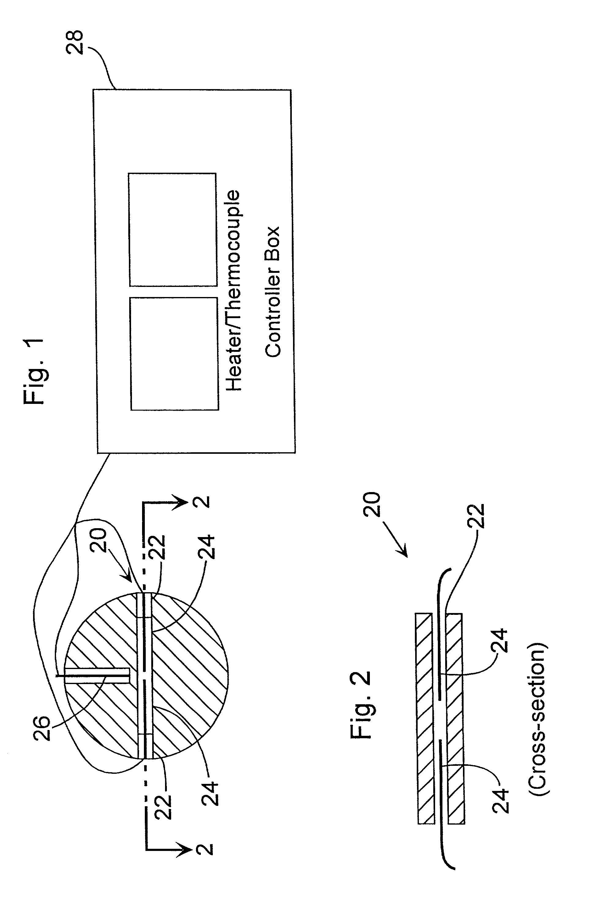
[0024]Embodiment With a Heated Upper, Lower and Side Electrodes and Other Heated Surfaces:

[0025]Reactor embodiment of the present invention can include heated electrode, deposition shield and / or other surfaces. By way of example only, FIGS. 1 and 2 depict plan and cross-sectional views of an upper electrode 20 for a reactor, and in particular of an etch reactor. The upper electrode has bores 22 provided therein which can receive heating elements 24. In this particular embodiment, two of the heating elements 24 are preferably cartridge heaters with an internal thermocouple. The third element 26 is a cartridge heater used as a thermocouple in order to sense the temperature. The cartridge heaters 24 and the cartridge heater 26 using a thermocouple are connected to a controller box 28 which uses the sensed temperature to maintain the level of heat generated by the cartridge heaters and thus the temperature of the upper electrode. In this preferred embodiment, the heaters are resistive t...


PUM

PropertyMeasurementUnit
Temperatureaaaaaaaaaa

Abstract

A reactor for processing semiconductor wafers with electrodes and other surfaces that can be one of heated, textured and/or pre-coated in order to facilitate adherence of materials deposited thereon, and eliminate the disadvantages resulting from the spaulding, flaking and/or delaminating of such materials which can interfere with semiconductor wafer processing.

Description

CROSS-REFERENCE[0001]This application is a continuation of Ser. No. 09 / 453,842, filed Dec. 2, 1999.[0002]Cross-referenced and incorporated by reference are U.S. Patent Applications entitled A METHOD FOR MINIMIZING THE CRITICAL DIMENSION GROWTH OF A FEATURE ON A SEMICONDUCTOR WAFER filed on Nov. 19, 1997, and with Ser. No. 08 / 974,089, issued Apr. 4, 2000 as U.S. Pat. No. 6,046,116; and U.S. Patent Application entitled PLASMA REACTOR WITH A DEPOSITION SHIELD, filed on Dec. 5, 1997, and with Ser. No. 08 / 985,730, now abandoned; and U.S. Patent Application entitled PLASMA REACTOR WITH A DEPOSITION SHIELD filed on Dec. 1, 1998, and with Ser. No. 09 / 204,020, issued Dec. 28, 1999 as U.S. Pat. No. 6,006,694.FIELD OF THE INVENTION[0003]The present invention is directed to reactors and in particular reactors for processing objects with films such as semiconductor wafers.BACKGROUND OF THE INVENTION[0004]During fabrication of semiconductor chips, wafers are processed in reactors which can accomp...

Claims


Application Information

Patent Timeline
IPC IPC(8): H01L21/302C23F1/00C23C16/46C23C16/44H01J37/32H01L21/00H01L21/3065
CPCC23C16/4404H01J37/32009H01J37/32724H01L21/67069H01L21/67098
Inventor DEORNELLAS, STEPHENJERDE, LESLIEOLSON, KURT
Owner OEM GRP LLC
Why Eureka
Try Eureka