Organic electroluminescent device, manufacturing method thereof, and electronic apparatus

a technology of electroluminescent devices and manufacturing methods, applied in the direction of discharge tube luminescnet screens, natural mineral layered products, etc., can solve the problems of less reliable polymer organic el elements than low-molecular organic el elements, and achieve the effect of long driving li

Inactive Publication Date: 2008-11-11
SEIKO EPSON CORP
View PDF18 Cites 4 Cited by
  • Summary
  • Abstract
  • Description
  • Claims
  • Application Information

AI Technical Summary

Benefits of technology

[0005]An advantage of the invention is to provide an organic electroluminescent element that has a long driving life.
[0006]Another advantage of the invention is to provide an electronic apparatus including the above-mentioned organic electroluminescent element.
[0007]An organic electroluminescent device according to one aspect of the invention includes an anode, a cathode, and a light-emitting functional portion sandwiched between the anode and the cathode. The light-emitting functional portion includes a light-emitting part, an electron injection and transport part, and a hole injection and transport part.
[0008]In this aspect, the anode is in contact with a titanium oxide particle thin layer.
[0009]An organic electroluminescent device according to another aspect of the invention also includes an anode, a cathode, and a light-emitting functional portion sandwiched between the anode and the cathode, and the light-emitting functional portion includes a light-emitting part, an electron injection and transport part, and a hole injection and transport part.
[0010]In this aspect, the cathode is in contact with a titanium oxide particle thin layer.

Problems solved by technology

Polymer organic EL elements are less reliable than low-molecular organic EL elements.

Method used


Image

  • Organic electroluminescent device, manufacturing method thereof, and electronic apparatus
  • Organic electroluminescent device, manufacturing method thereof, and electronic apparatus
  • Organic electroluminescent device, manufacturing method thereof, and electronic apparatus

Examples


Embodiment Construction

1. Organic EL Device

[0026]Examples in which a method for manufacturing a multilayered body is applied to an organic EL device will now be shown as embodiments of the present invention. In this example, at least one of an organic light-emitting layer, hole injection layer, and electron injection layer corresponds to the light-emitting functional part.

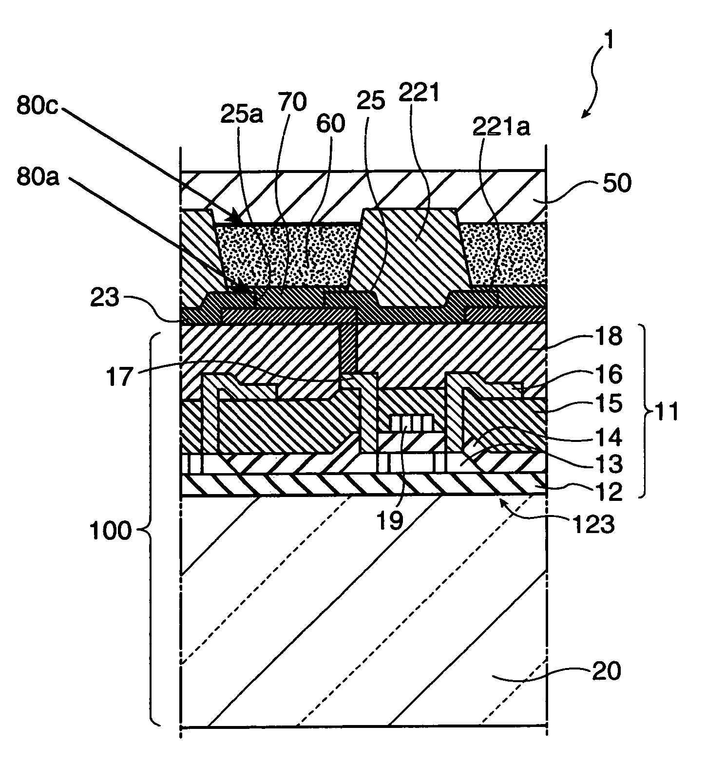
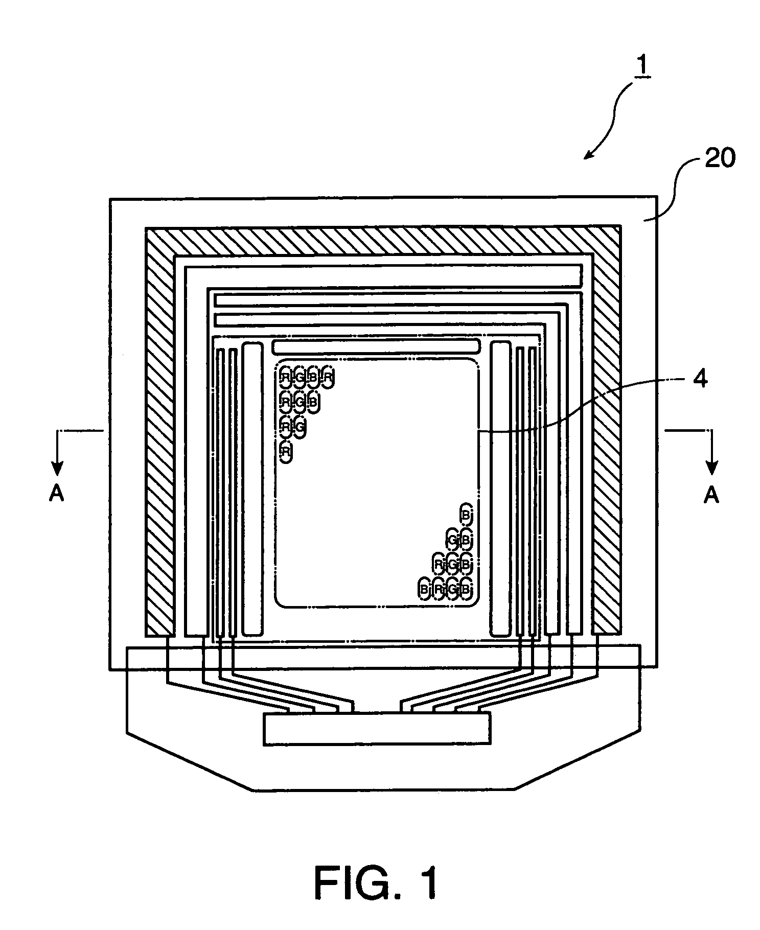
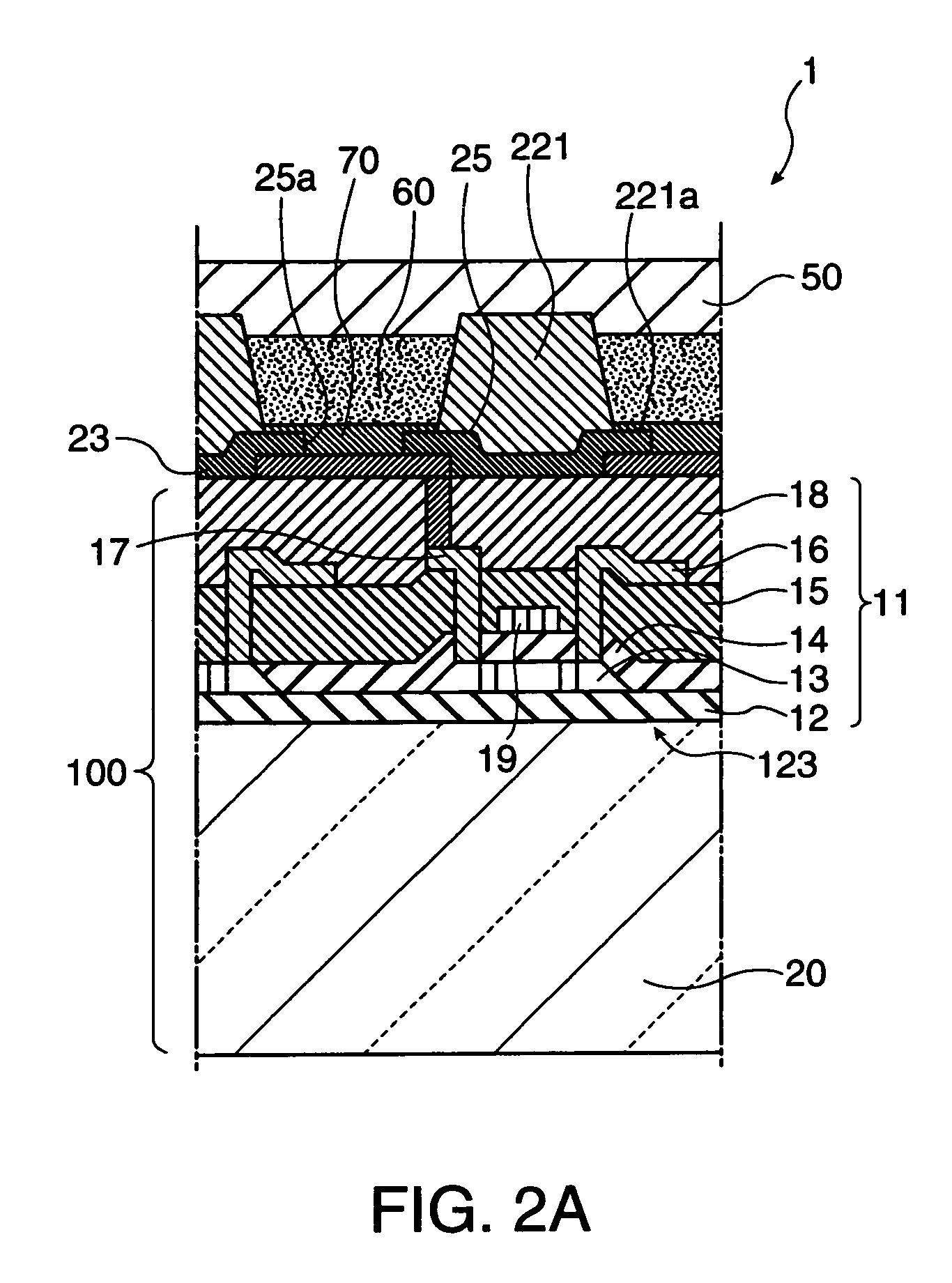
[0027]Referring to FIGS. 1 and 2, an example of an organic EL device according to one embodiment of the invention is described. FIG. 1 is a plan view schematically showing an organic EL device 1. FIG. 2 is a schematic sectional view along line A-A of FIG. 1.

[0028]Referring to FIG. 1, the organic EL device 1 includes dots each of which emits red (R), green (G) or blue (B) light in an actual display area 4 to display full color.

[0029]As shown in FIG. 2A, the organic EL device 1 of the present embodiment has a bottom-emission structure. This structure provides light from a substrate 20 side, and therefore the substrate 20 is made of a trans...


PUM

PropertyMeasurementUnit
thicknessaaaaaaaaaa
temperatureaaaaaaaaaa
thicknessaaaaaaaaaa

Abstract

An organic electroluminescent device, comprising an anode;
    • a cathode; and a light-emitting functional portion sandwiched between the anode and the cathode, the light-emitting functional portion including a light-emitting part, an electron injection and transport part, and a hole injection and transport part; the anode being in contact with a titanium oxide particle thin layer.

Description

[0001]This application claims the benefit of Japanese patent Application No. 2004-240449, filed Aug. 20, 2004. The entire disclosure of the prior application is hereby incorporated by reference herein in its entirety.BACKGROUND[0002]The present invention relates to a method for manufacturing an organic electroluminescent device using a liquid-phase process, an organic electroluminescent device manufactured by the method, and an electronic apparatus.[0003]Organic electroluminescent (EL) devices using organic matters have been developed as self light-emitting displays that can replace liquid crystal displays at an accelerated rate in recent years. Examples of methods for manufacturing such organic EL devices that have been proposed include providing low molecules by a vapor-phase process such as evaporation and providing polymers by a liquid-phase process. See Applied Physics Letters, Vol. 51 (12), 21 Sep. 1987, p. 913, and Applied Physics Letters, Vol. 71 (1), 7 Jul. 1997, p. 34, for...

Claims


Application Information

Patent Timeline
Patent Type & Authority Patents(United States)
IPC IPC(8): H01L51/50B05D5/12
CPCH01L51/5088H01L51/5092H01L51/0003Y10S428/917Y10T428/256H10K71/12H10K50/171H10K50/17H05B33/26
Inventor MORII, KATSUYUKISAKAI, HIROFUMITOYODA, NAOYUKI
Owner SEIKO EPSON CORP
Why Eureka
Try Eureka