Electron beam exposure apparatus, electron beam exposure method and method of manufacturing semiconductor device
an electron beam and exposure method technology, applied in the field of electron beam exposure apparatus and electron beam exposure method, can solve the problems of reducing drawing throughput, shortening drawing time, and reducing the size of the cell in the devi
- Summary
- Abstract
- Description
- Claims
- Application Information
AI Technical Summary
Problems solved by technology
Method used
Image

Examples
Embodiment Construction
[0038]One embodiment of the present invention will be described below with reference to the drawings.
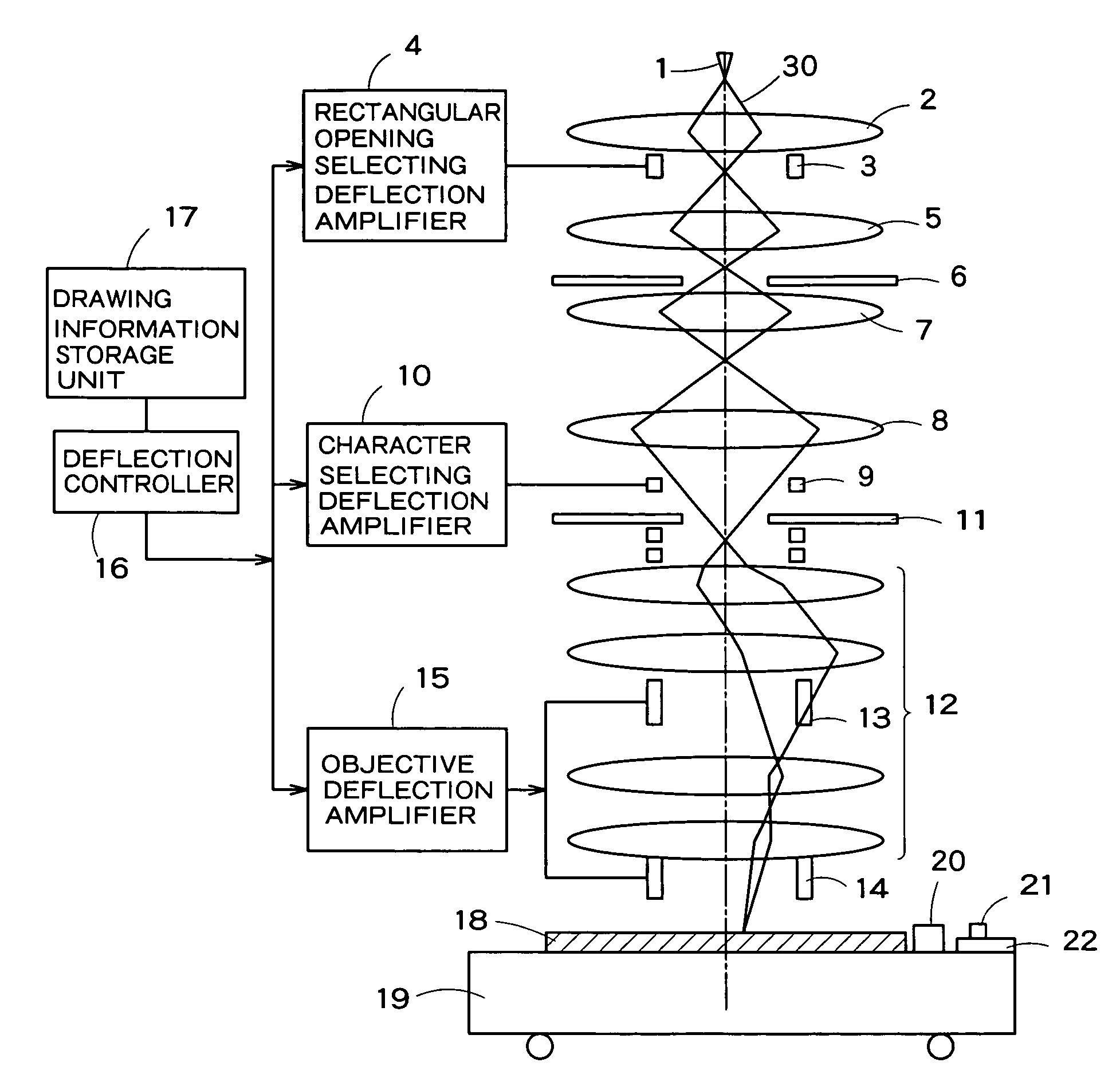
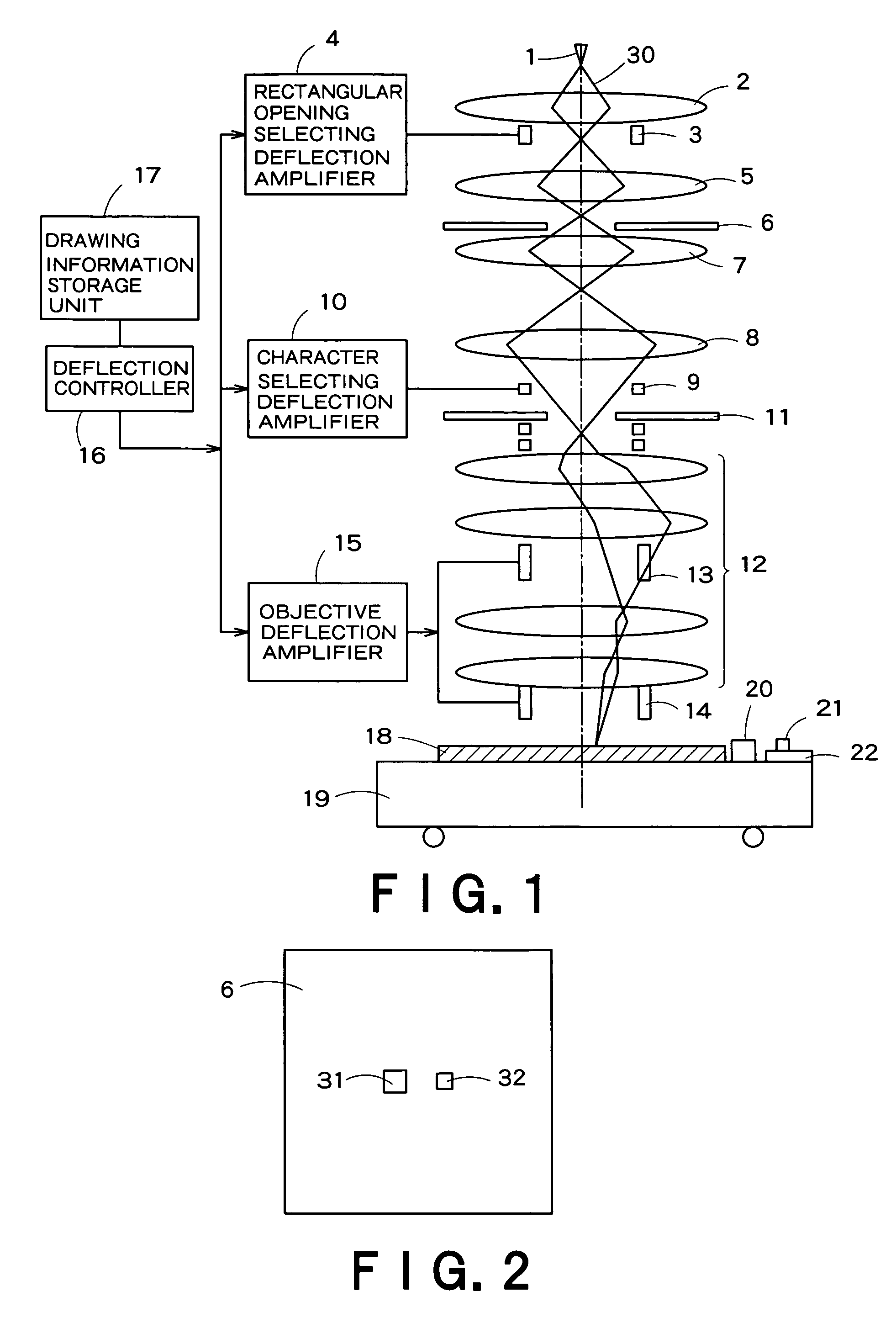
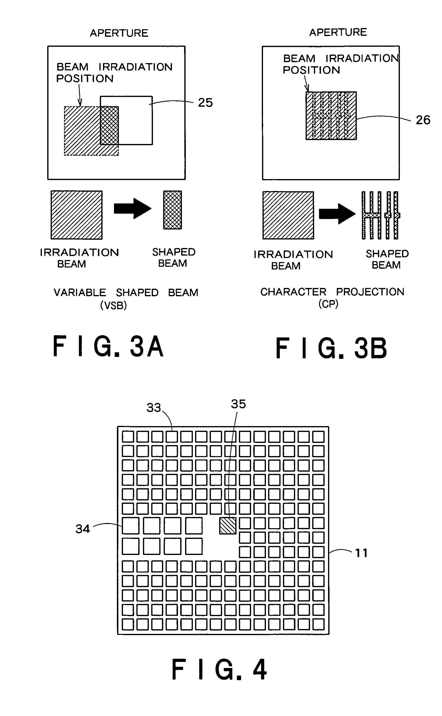
[0039]FIG. 1 is a view showing a schematic configuration of an electron beam exposure apparatus according to one embodiment of the present invention. The electron beam exposure apparatus of FIG. 1 includes an electron gun 1, a first condenser lens 2, a rectangular opening selection deflector 3, a rectangular opening selecting deflection amplifier 4, a second condenser lens 5, a first shaping aperture 6, a first projection lens 7, a second projection lens 8, a character selection deflector 9, a character selecting deflection amplifier 10, a second shaping aperture 11, an imaging lens system 12, an objective deflection amplifier 15 controlling a primary objective deflector 13 and a secondary objective deflector 14 of the lens system 12, a deflection controller 16, a drawing information storage unit 17 storing information relating to a circuit pattern drawing method, a movable stage 19 ...
PUM
 Abstract
Description
Claims
Application Information
 - R&D Engineer
- R&D Manager
- IP Professional
- Industry Leading Data Capabilities
- Powerful AI technology
- Patent DNA Extraction
Browse by: Latest US Patents, China's latest patents, Technical Efficacy Thesaurus, Application Domain, Technology Topic.
© 2024 PatSnap. All rights reserved.Legal|Privacy policy|Modern Slavery Act Transparency Statement|Sitemap