Illumination system for illuminating a mask in a microlithographic exposure apparatus

A lighting system and exposure device technology, applied in the field of lighting systems, can solve problems such as array production and reliability failing to meet requirements, arrays being expensive, etc.

Active Publication Date: 2010-03-10
CARL ZEISS SMT GMBH
View PDF8 Cites 18 Cited by
  • Summary
  • Abstract
  • Description
  • Claims
  • Application Information

AI Technical Summary

Problems solved by technology

However, the production and reliability of such arrays has not been satisfactory, and even if...

Method used


Image

  • Illumination system for illuminating a mask in a microlithographic exposure apparatus
  • Illumination system for illuminating a mask in a microlithographic exposure apparatus
  • Illumination system for illuminating a mask in a microlithographic exposure apparatus

Examples


Embodiment Construction

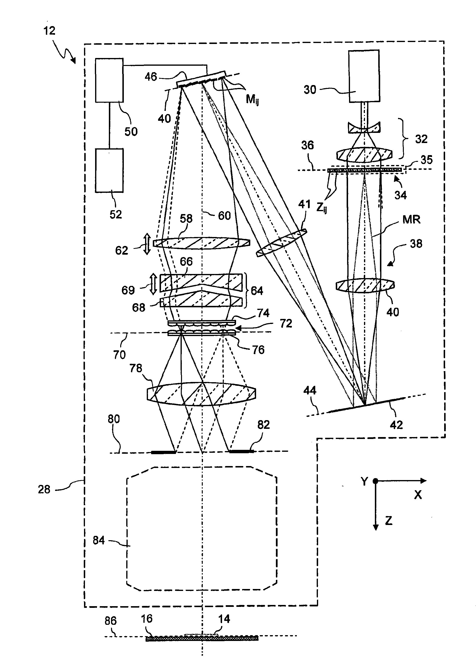
[0056] 1. Overall structure of projection exposure equipment

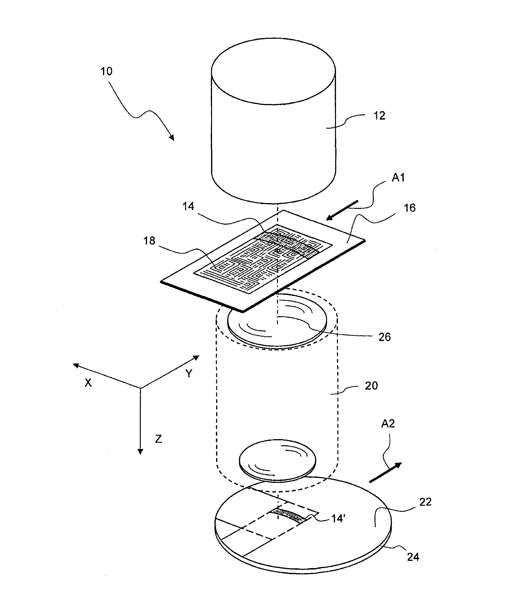
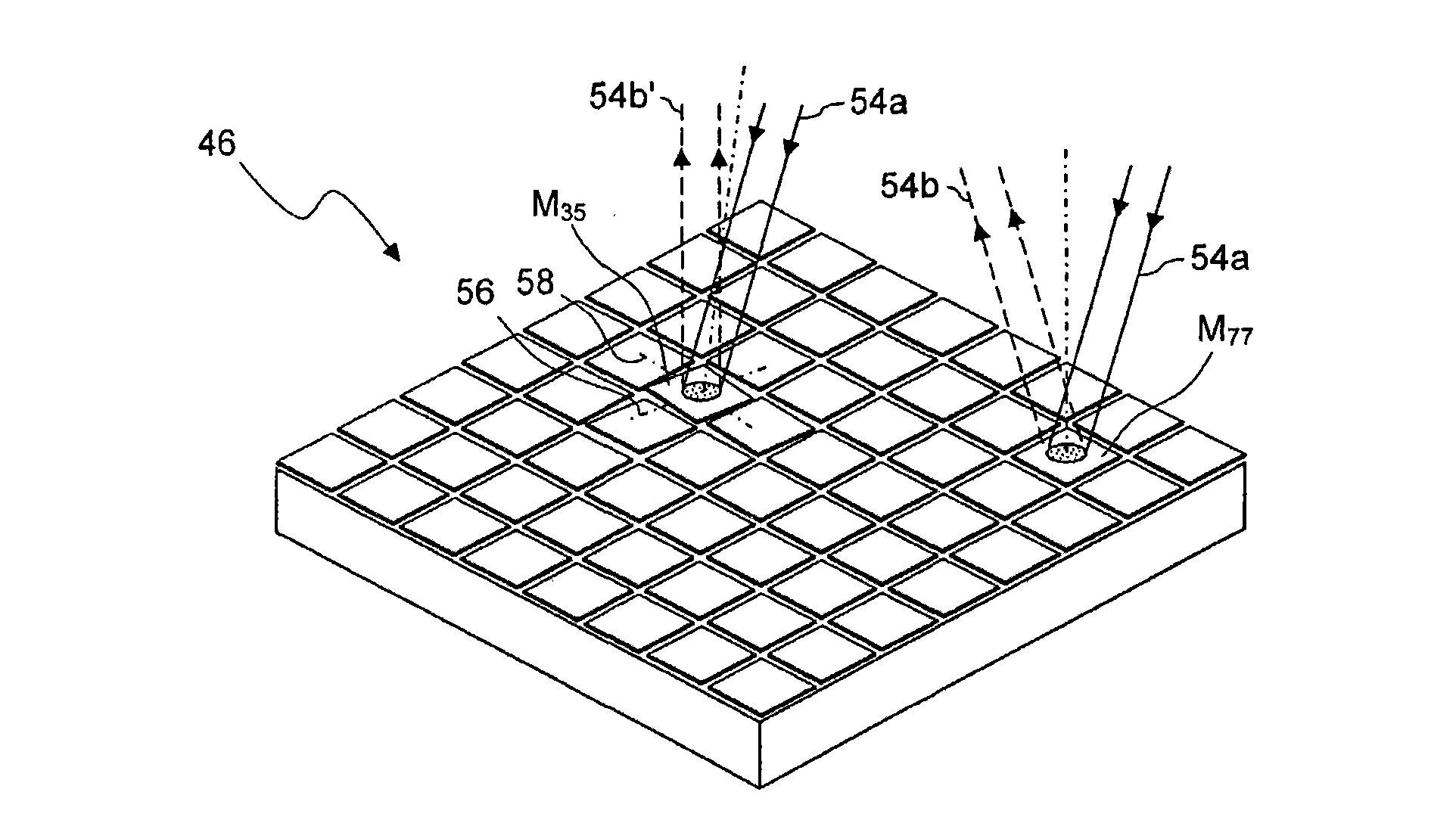
[0057] figure 1 is a perspective and highly simplified view of projection exposure equipment used in the fabrication of integrated circuits and other microstructured components. The projection exposure apparatus comprises an illumination system comprising a light source 12 generating projection light and illumination optics converting the projection light into a projection beam with carefully defined characteristics. The projection beam illuminates an area 14 on the mask 16 containing minimal structures 18, the illuminated area 14 having approximately the shape of an annulus. However, other shapes of the illuminated area 14 , for example rectangular, are also conceivable.

[0058] The projection objective 20 images the structures 18 in the illuminated area 14 onto a photosensitive layer 22 applied to a substrate 24, for example a photoresist material. A substrate 24 , which may be formed from a silicon wafer, is...


PUM


Abstract

An illumination system for illuminating a mask in a microlithographic exposure apparatus has an optical axis and a pupil surface. The system can include an array of reflective or transparent beam deflection elements such as mirrors. Each deflection element can be adapted to deflect an impinging light ray by a deflection angle that is variable in response to a control signal. The beam deflection elements can be arranged in a first plane. The system can further include an optical raster element, which includes a plurality of microlenses and/or diffractive structures. The beam deflection elements), which can be arranged in a first plane, and the optical raster element, which can be arranged in a second plane, can commonly produce a two-dimensional far field intensity distribution. An opticalimaging system can optically conjugate the first plane to the second plane.

Description

[0001] Cross References to Related Applications [0002] This application claims the benefit of US Provisional Application Nos. 60 / 913,962 and 60 / 913,956, both filed April 25, 2007, under 35 U.S.C 119. technical field [0003] The present invention generally relates to an illumination system for illuminating a mask in a microlithographic exposure apparatus. More specifically, the present invention relates to such an illumination system comprising an array of reflective elements, which may be realized as a microelectro-mechanical system (MEMS), in particular a digital micromirror device (DMD). Background technique [0004] Microlithography (also called optical lithography or just photolithography) is a technique used to fabricate integrated circuits, liquid crystal displays, and other microstructured devices. More specifically, the process of microlithography combined with an etching process is used to pattern features in a thin film stack formed on a substrate (eg, a silico...

Claims


Application Information

Patent Timeline
IPC IPC(8): G03F7/20
CPCG03F7/70158G03F7/70116G03F7/70216
Inventor 马库斯·德冈瑟保罗·格劳普纳于尔根·费希尔
Owner CARL ZEISS SMT GMBH
Why Eureka
Try Eureka