System and process for measuring strain in materials at high spatial resolution

a technology of high spatial resolution and system and process, applied in the field of electron microscopy system and process, can solve the problems of weak changes in the beam intensity distribution, the accuracy required for some measurements, which can be less than 0.1% strain, and the inability to achieve the accuracy of those methods, so as to reduce the dynamical diffraction

Active Publication Date: 2015-03-19
APPFIVE
View PDF2 Cites 18 Cited by
  • Summary
  • Abstract
  • Description
  • Claims
  • Application Information

AI Technical Summary

Benefits of technology

[0009]A process for measuring strain is provided that includes placing a sample of a material into a TEM as a sample. The TEM is energized to create a small electron beam with an incident angle to the sample. Electrical signals are generated that control multiple beam deflection coils and image deflection coils of the TEM. The beam deflection control signals cause the angle of the incident beam to change in a cyclic time-dependent manner. A first diffraction pattern from the sample material that shows dynamical diffraction effects is observed and then one or more of the beam deflection coil control signals are adjusted to reduce the dynamical diffraction effects. One or more of the image deflection coil control signals are then adjusted to remove any motion of the diffraction pattern. A diffraction pattern is then collected from a strain

Problems solved by technology

But those methods suffer from some significant systematic errors that result from strong changes in the beam intensity distribution that are not due to strain (see the description of dynamical diffraction below).
The precision required for some measurements, which can be less than 0.1% strain, is often not attainable with those methods.
The main systematic errors in measuring spot positions from conventional NBD patterns, and therefore in calculating strain within a material, arise from the fact that the diffr

Method used


Image

  • System and process for measuring strain in materials at high spatial resolution
  • System and process for measuring strain in materials at high spatial resolution
  • System and process for measuring strain in materials at high spatial resolution

Examples


Embodiment Construction

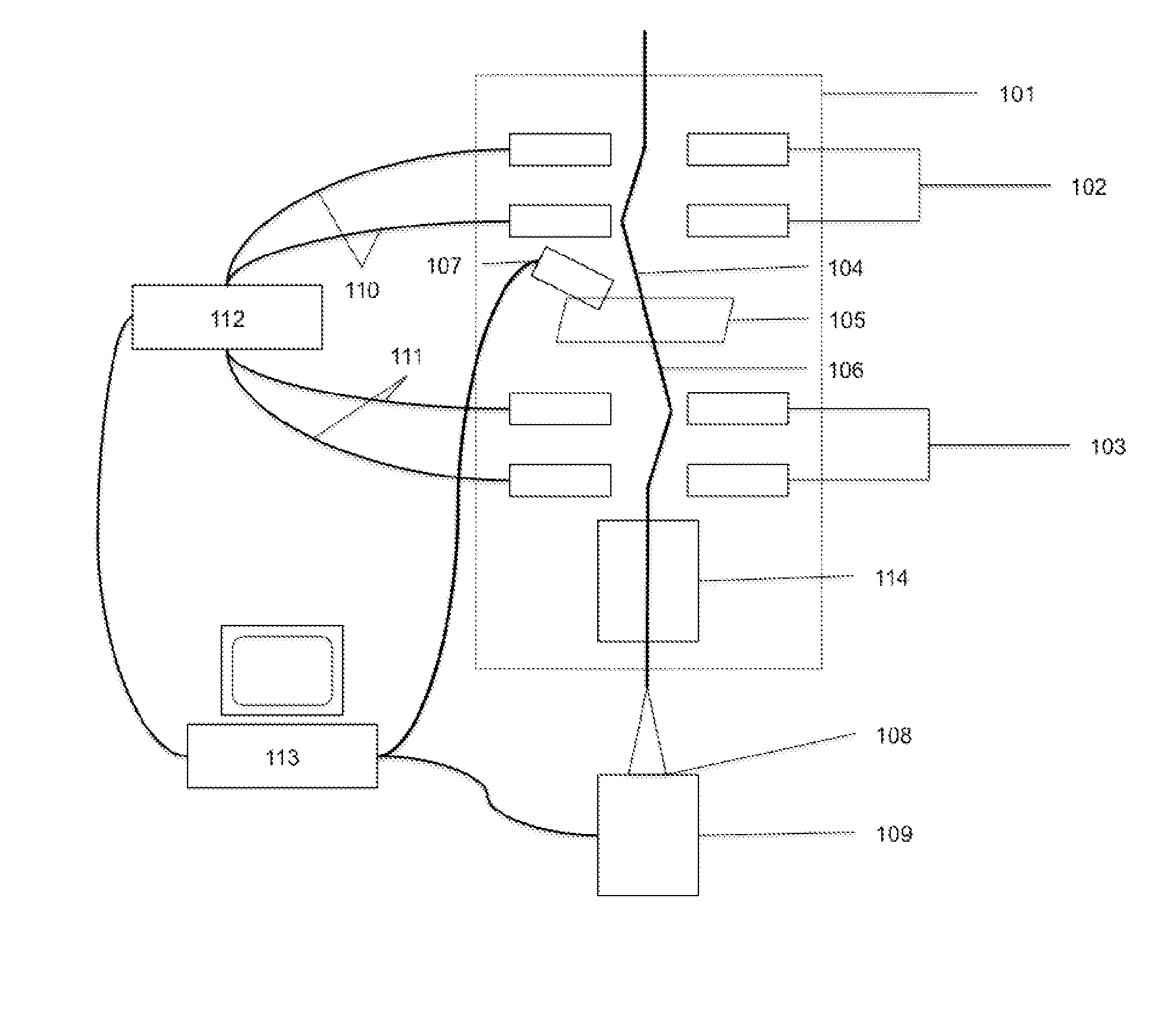
[0014]The present invention has utility as a system and a process of performing PED in TEM. In one embodiment of the present invention, a TEM with an accelerating voltage between 20 kV and 1.5 MV is fitted with a device (the “Precession Device”) that applies signals to the TEM that produce a time-dependent change in the angle of the incident electron beam. The Precession Device also applies signals to the TEM to stop the motion of the diffraction patterns that is induced by the change of angle of the incident electron beam. In specific embodiments, the incident electron beam is a small diameter probe that produces NBD patterns and raster scanned (“STEM”) images. The TEM is also fitted in specific embodiments with a camera (the “Camera”) to record TEM images and / or diffraction patterns. A computer, through software running on the computer (the “Software”), controls various operational aspects of the TEM, the Precession Device, and the Camera. The Software acquires PED patterns using ...


PUM


Abstract

A process for measuring strain is provided that includes placing a sample of a material into a TEM as a sample. The TEM is energized to create a small electron beam with an incident angle to the sample. Electrical signals are generated that control multiple beam deflection coils and image deflection coils of the TEM. The beam deflection control signals cause the angle of the incident beam to change in a cyclic time-dependent manner. A first diffraction pattern from the sample material that shows dynamical diffraction effects is observed and then one or more of the beam deflection coil control signals are adjusted to reduce the dynamical diffraction effects. One or more of the image deflection coil control signals are then adjusted to remove any motion of the diffraction pattern. A diffraction pattern is then collected from a strained area of the material after the adjusting step, and the strain is then determined from a numerical analysis of the strained diffraction pattern compared to a reference diffraction pattern from an unstained area of the material.

Description

FIELD OF THE INVENTION[0001]The application claims priority benefit of U.S. Provisional Application Ser. No. 61 / 608,413 filed 8 Mar. 2013; the contents of which are hereby incorporated by reference.FIELD OF THE INVENTION[0002]The invention in general relates to a system and process for electron microscopy to determine the local strain in materials, and in particular to precession electron diffraction and the generation of position-resolved strain distributions from samples subjected to electron microscopy.BACKGROUND[0003]Electron diffraction patterns offer the ability to measure the lattice parameters of crystalline materials. A small (<10 nanometer (nm)) focused electron probe can be produced by a transmission electron microscope (“TEM”), and the probe can be positioned in two dimensions to a precision of better than 1 nm. The probe is amenable to being moved quickly (<1 ms) to any position over a large (>1 μm) field of view. For electron-transparent samples, it is therefo...

Claims


Application Information

Patent Timeline
IPC IPC(8): G01N23/225H01J37/26G01N3/02
CPCG01N23/2251G01N3/02H01J2237/2448H01J2237/2602H01J2237/15H01J37/261H01J37/26G01N23/20058H01J37/2955H01J2237/24585H01J2237/2802
Inventor WEISS, JON KARLDARBAL, AMITH D.NARAYAN, RAMAN D.KIM, STEVEN T.NICOLOPOULOS, STAVROS
Owner APPFIVE
Why Eureka
Try Eureka