Magnetoresistive element, magnetic memory cell, and magnetic memory device
a technology of magnetic memory cell and magnetic memory device, which is applied in the direction of galvano-magnetic devices, digital storage, instruments, etc., can solve the problems of unstable magnetic direction in the free magnetic direction layer for storing information, inability to hold information to be recorded, etc., to achieve stably writing and hold written information
- Summary
- Abstract
- Description
- Claims
- Application Information
AI Technical Summary
Benefits of technology
Problems solved by technology
Method used
Image
Examples
first embodiment
[0074]First, with reference to FIGS. 1 to 7, the configuration of a magnetic memory device according to a first embodiment of the invention will be described.
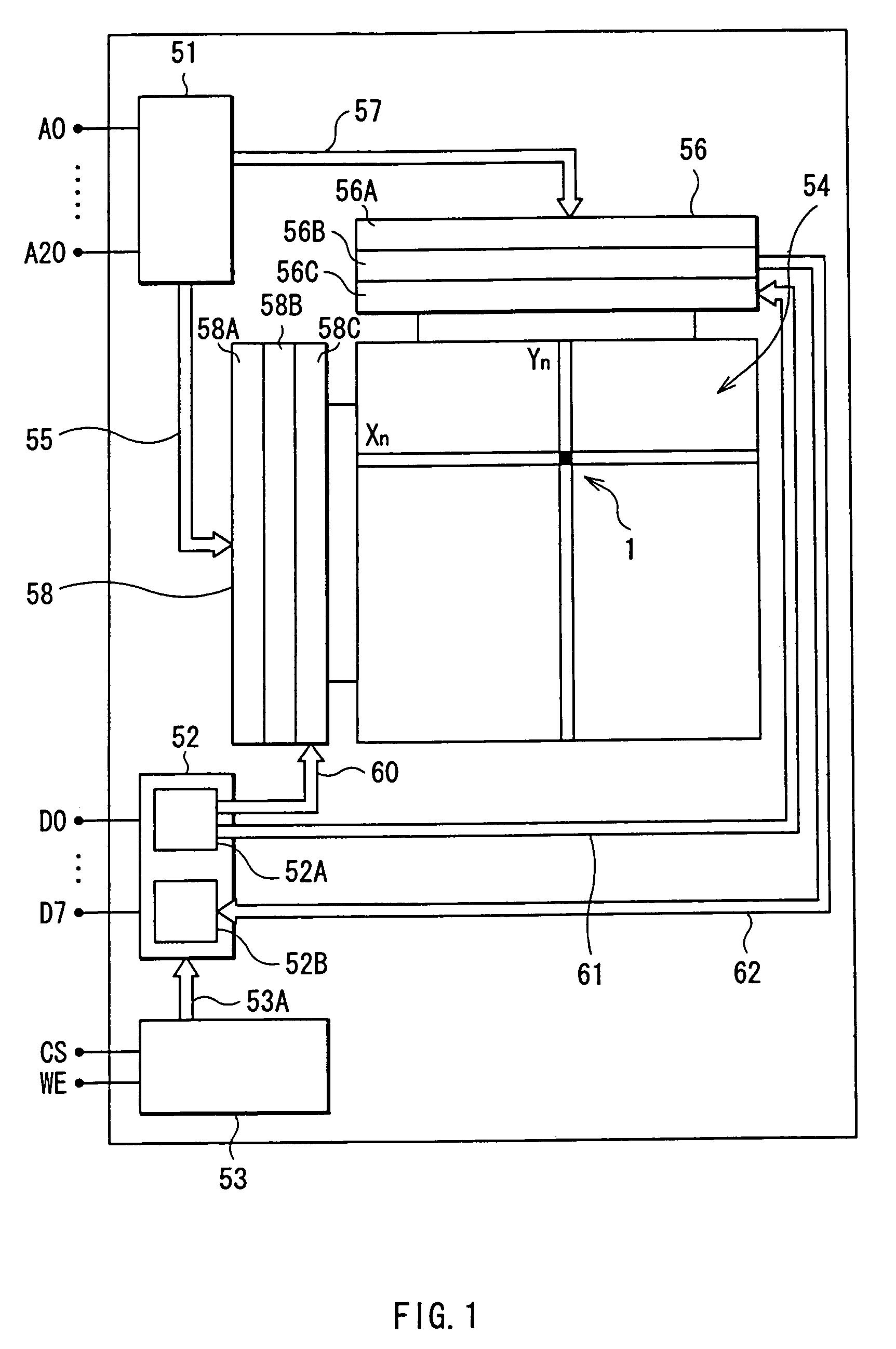
[0075]FIG. 1 is a conceptual diagram showing a general configuration of a magnetic memory device in the embodiment. The magnetic memory device has an address buffer 51, a data buffer 52, a control logic part 53, a memory cell group 54, a first drive control circuit part 56, a second drive control circuit part 58, external address input terminals A0 to A20, and external data terminals D0 to D7.
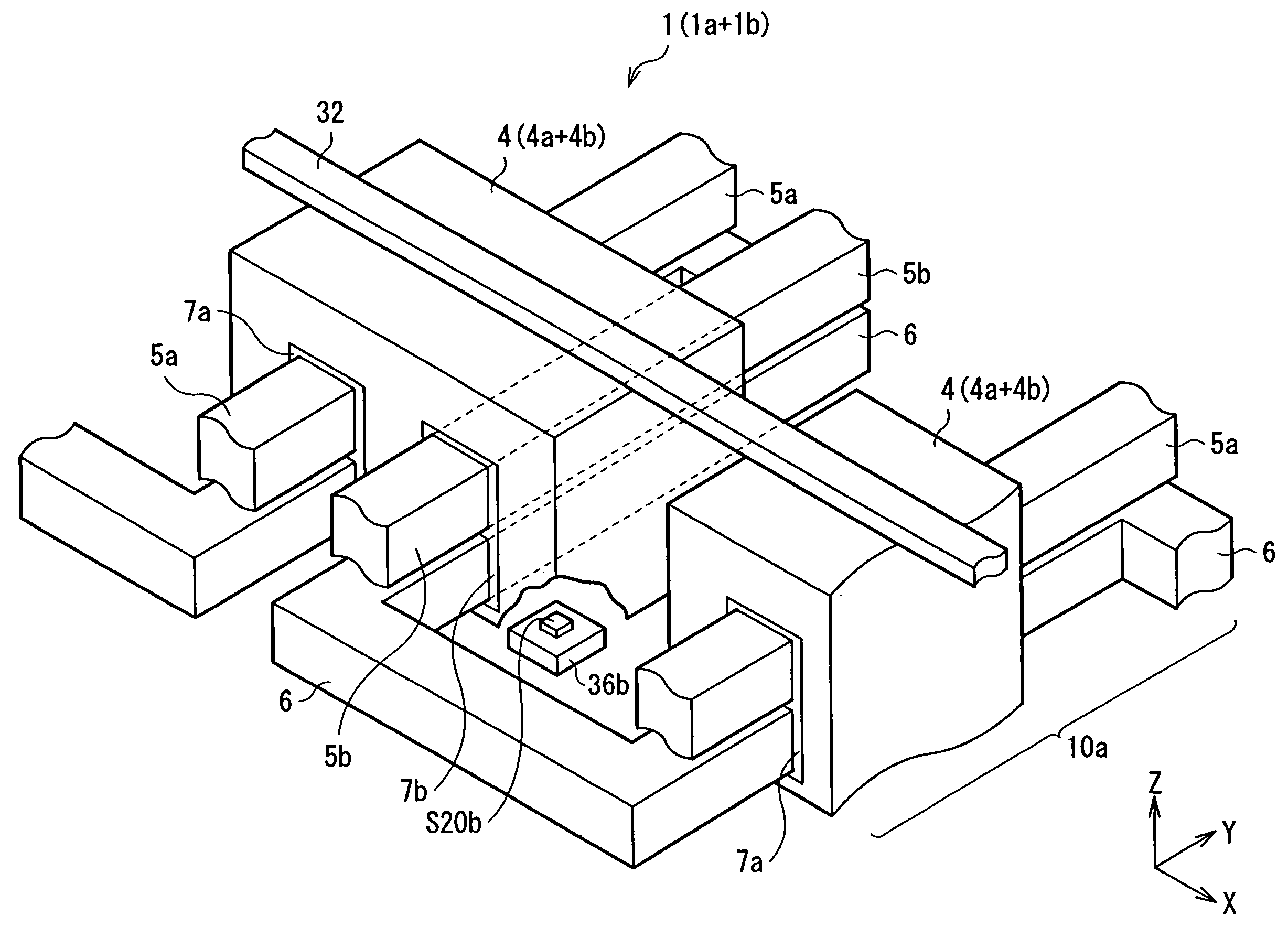
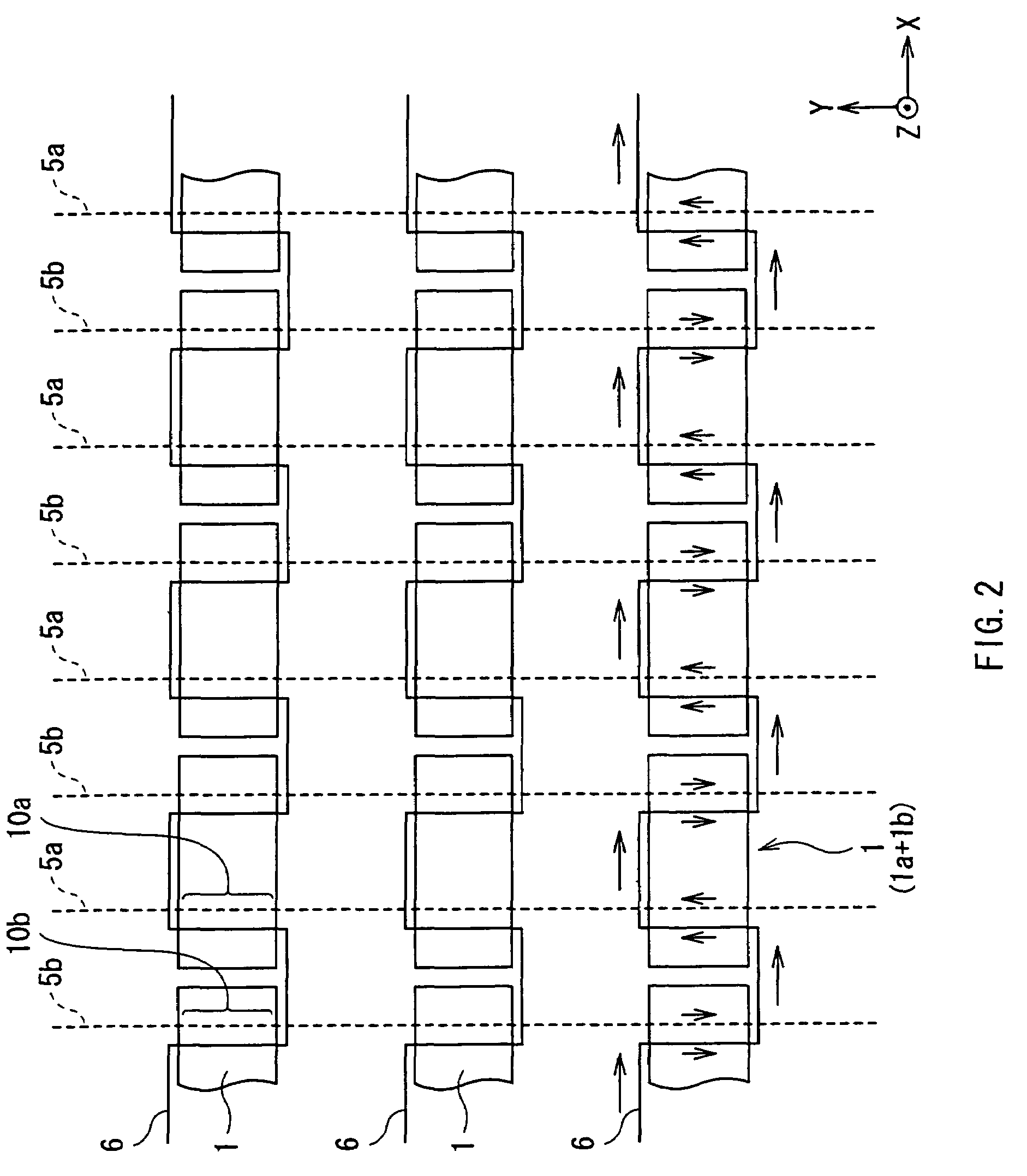
[0076]The memory cell group 54 has a matrix structure in which a number of memory cells 1 each having a pair of tunneling magneto-resistive elements (hereinbelow, called TMR elements) are arranged in a word line direction (X direction) and a bit line direction (Y direction) which are orthogonal to each other. The memory cell 1 is the minimum unit for storing data in the magnetic memory device and is a concrete example corresponding to a “m...
second embodiment
[0142]A magnetic memory device of a second embodiment of the invention will now be described with reference to FIGS. 28A and 28B and FIGS. 29A and 29B.
[0143]FIGS. 28A and 28B show a sectional configuration of a memory cell 121 in a magnetic memory device of the second embodiment, which corresponds to the memory cell 1 in FIGS. 5A and 5B of the first embodiment. In FIGS. 28A and 28B, the same reference numerals are assigned to components substantially the same as those shown in FIGS. 5A and 5B.
[0144]In the following, with respect to the configuration of the magnetic memory device of the second embodiment and a method of manufacturing the magnetic memory device, the points different from the first embodiment will be mainly described and the other description be omitted appropriately.
[0145]In the memory cell 1 of the first embodiment, each of the pair of the TMR elements 1a and 1b has: the magnetic yokes 4a and 4b constructed so as to surround the whole periphery of the write bit lines...
PUM
 Abstract
Description
Claims
Application Information


