
Continuous phase frequency shift keying modulation during wireless transmissions in a closed system while minimizing power consumption

a technology of closed system and frequency shift, applied in frequency-modulated carrier systems, digital transmissions, therapy, etc., can solve the problems of phase discontinuities in fsk modulated output signals, wireless transmissions less robust, negative impact on the demodulation of recovered signals, etc., to minimize energy consumption

Inactive Publication Date: 2008-11-11
MEDOS INT SARL
View PDF17 Cites 1 Cited by
  • Summary
  • Abstract
  • Description
  • Claims
  • Application Information

AI Technical Summary

Benefits of technology

[0007]Another object of the present invention to provide circuitry for employing CPFSK modulation while minimizing power consumption.
[0008]Yet another object of the present invention is to employ CPFSK modulation so as to increase the robustness of transmission of the demodulated signal therefrom.
[0009]Still another object of the present invention is to transmit a CPFSK modulated signal during uplink wireless transmission from an internal device to an external device of a closed system while eliminating the need for an active emitter on the implant side.
[0010]Continuous phase frequency shift keying modulation is employed during wireless transmission from an internal device to an external device to increase robustness of transmissions. The continuous phase frequency shift keying processor receives as input an incoming data stream and includes a timer for toggling its output between a first predetermined frequency and a second predetermined frequency on a predetermined time period basis based on the logical state of each bit in the incoming data stream. For a portion of time while the counter or timer of the CPFSK processor is counting down the predetermined time period associated with the detected logic state of a particular bit of the incoming data signal at least some of the other circuitry, preferably all of the other circuitry of the processor, is toggled to a sleep mode in which power is cut off thereby minimizing power consumption by the processor during this interim state.
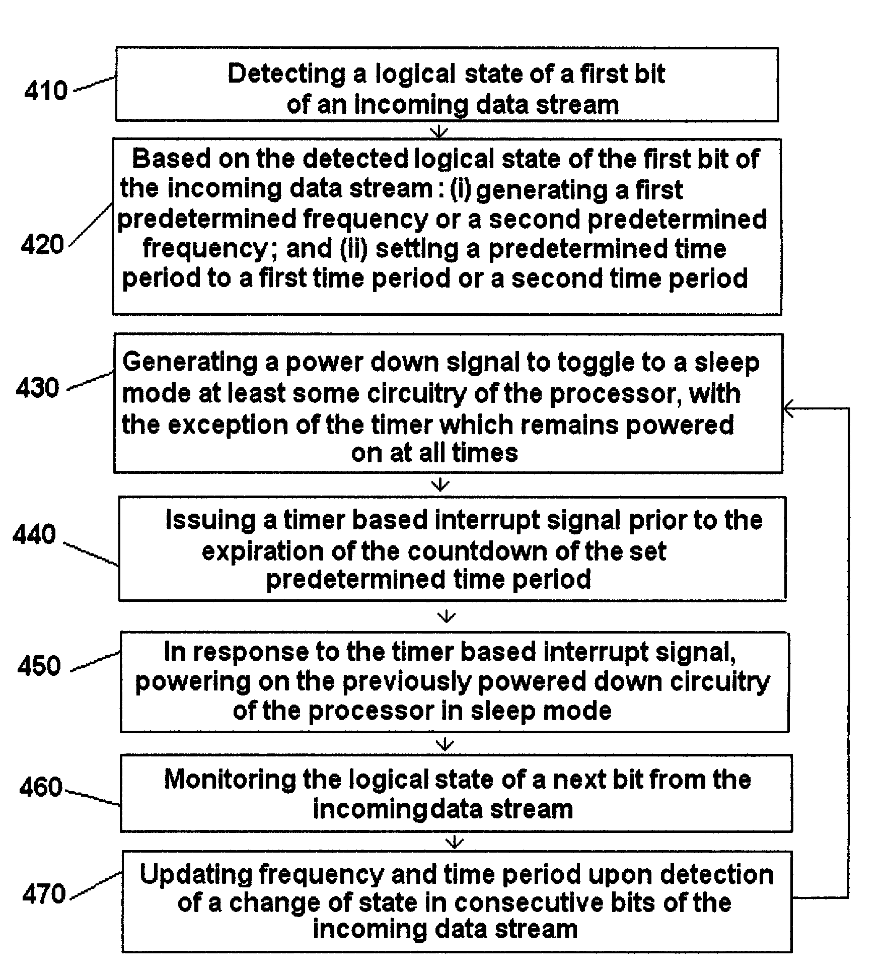
[0012]Furthermore, the invention is directed to a method for minimizing energy consumption of a continuous phase frequency shift keying modulation processor for use in a closed system, as described in the preceding paragraph. The method includes the steps of toggling of an output signal of the continuous phase frequency shift keying modulation processor between a first predetermined frequency and a second predetermined frequency on a predetermined time period basis based on a logical state of each bit in an incoming data stream to the continuous phase frequency shift keying modulation processor. Specifically, initially a logical state of a first bit of the incoming data signal to the internal device is detected. Based on the detected logical state of the first bit of the incoming data signal: (i) a continuous phase frequency shift keying encoded output signal is generated at one of a first predetermined frequency or a second predetermined frequency; and (ii) a predetermined time period of the timer of the continuous phase frequency shift keying processor is set to a first time period or a second time period. A power down signal is generated to toggle to a sleep mode at least some circuitry of the processor, while the timer associated with the continuous phase frequency shift keying processor remains powered on at all times. Prior to the expiration of the countdown by the timer of the set predetermined time period, preferably approximately half of the countdown of the set predetermined time period for the timer, a timer based interrupt signal is issued to power on the previously powered down circuitry of the processor in sleep mode. The logical state of a next bit from the incoming data stream is monitored. Upon detection of a change of logical state between consecutive bits of the incoming data stream, the frequency and associated time period for the timer are updated. This same process is repeated for each bit in the incoming data stream.
[0013]Yet another aspect of the invention is directed to a continuous phase frequency shift keying processor receiving as input an incoming data stream and producing a continuous phase frequency shift keying encoded output signal. The continuous phase frequency shift keying processor includes a timer for toggling the continuous phase frequency shift keying encoded output signal between a first predetermined frequency and a second predetermined frequency on a predetermined time period basis based on the logical state of each bit in the incoming data stream. The invention also relates to a method for minimizing energy consumption of a continuous phase frequency shift keying modulation processor, as described in the preceding paragraph.

Problems solved by technology

While generating the FSK modulated signal on either the implant or external side there is no way to ensure perfect synchronization (e.g., zero phase) when switching between the oscillators, thereby resulting in phase discontinuities in the FSK modulated output signal.
As a result of this discontinuity in phase of the FSK modulation signal the wireless transmission is less robust having a negative impact on the demodulation of the recovered signal.

Method used


Image

  • Continuous phase frequency shift keying modulation during wireless transmissions in a closed system while minimizing power consumption
  • Continuous phase frequency shift keying modulation during wireless transmissions in a closed system while minimizing power consumption
  • Continuous phase frequency shift keying modulation during wireless transmissions in a closed system while minimizing power consumption

Examples


Embodiment Construction

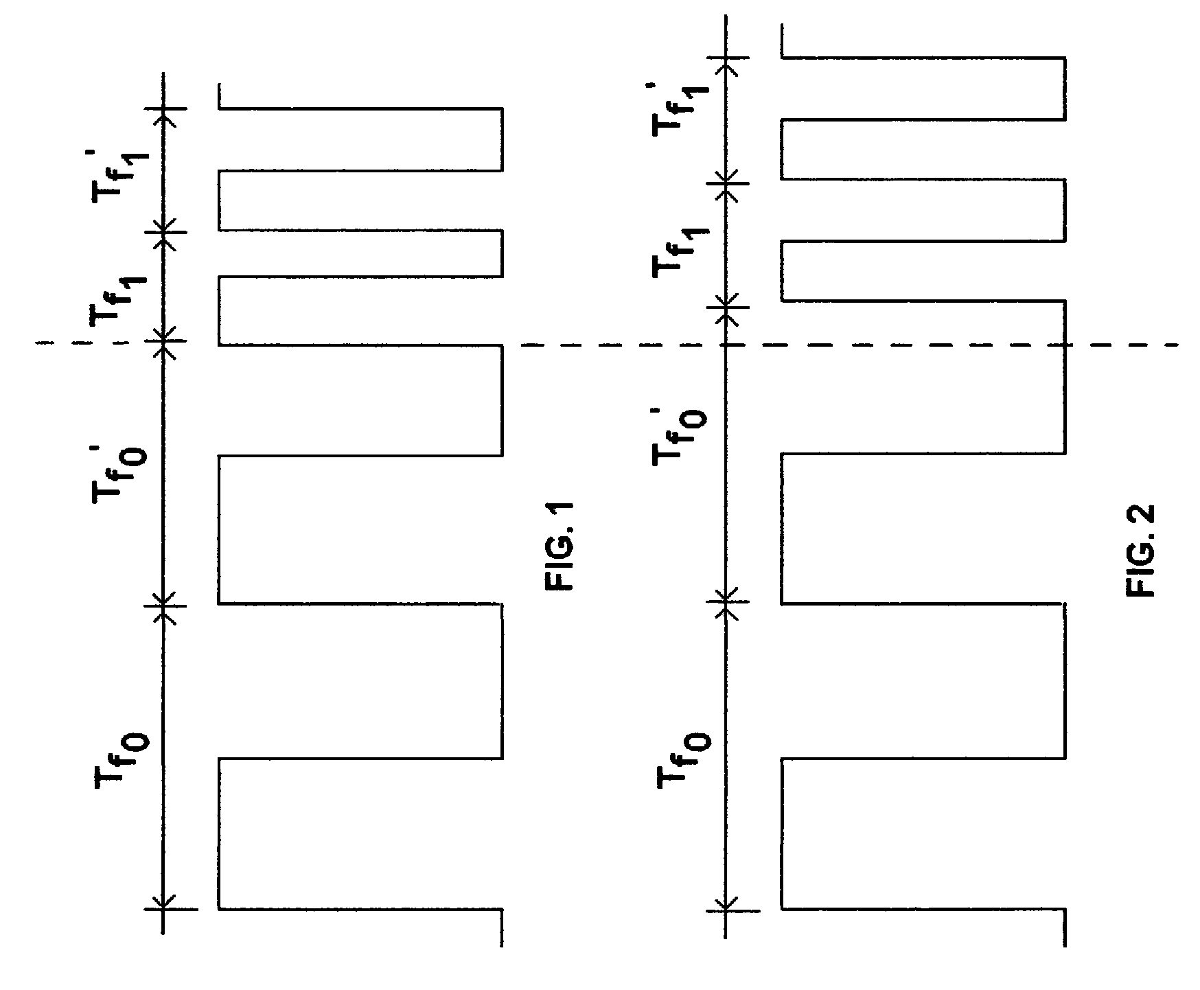
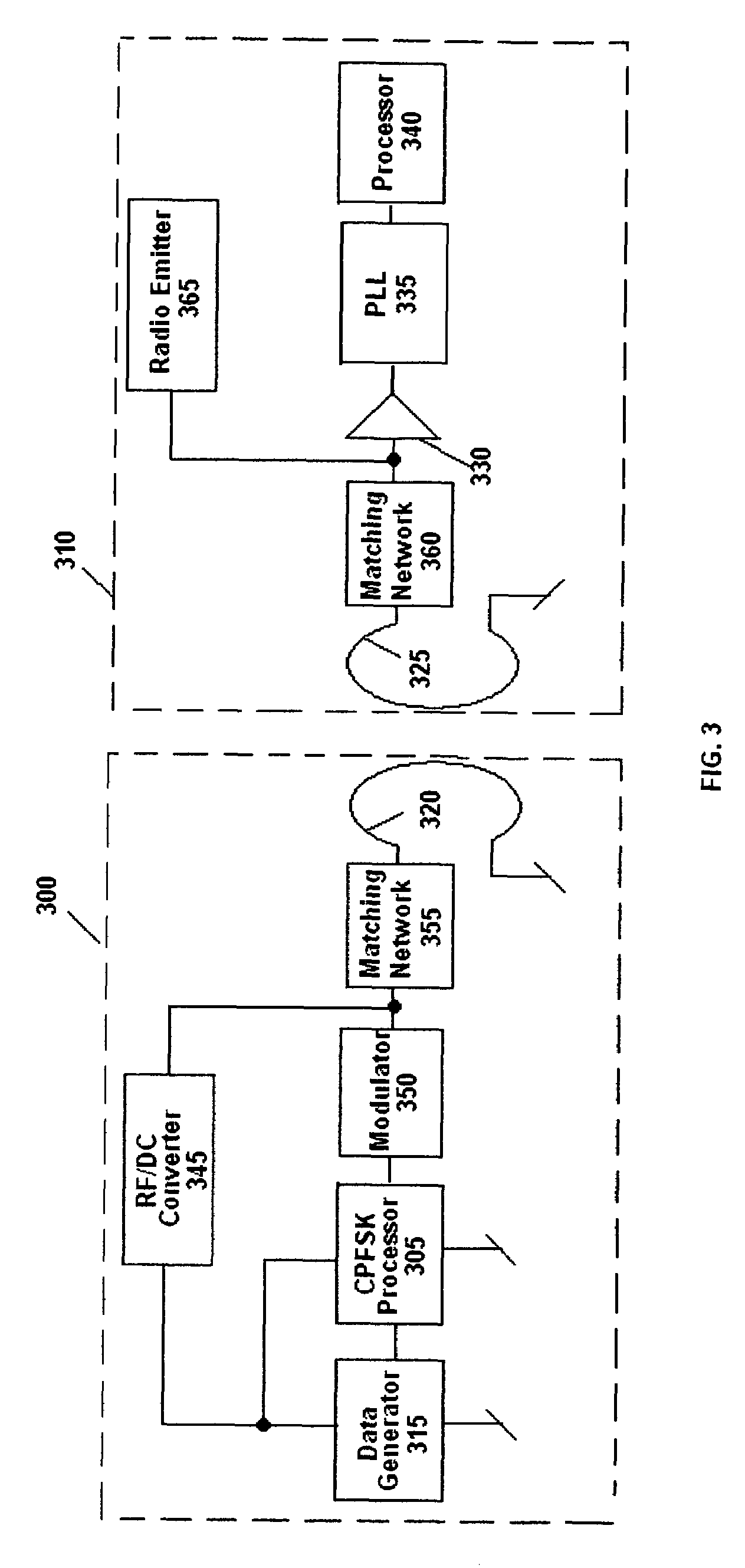
[0019]The present invention is directed to circuitry for generating in a closed system a continuous phase frequency shift keying (CPFSK) modulated signal using a dedicated wireless processor. One such application discussed in detail in the present invention is the use of the dedicated processor in an implantable medical device for generating a CPFSK modulated signal for uplink wireless transmission to an external device disposed outside the patient's body. It is, however, contemplated and within the intended scope of the present invention to be used for any type of wireless transmission. The use of zero phase crossover CFSK is particularly advantageous during wireless transmissions between devices in a closed system in that it (i) provides smoother transitions from high (e.g.,“1”) to low (e.g., “0”) bits, (ii) limits the radiated harmonics, and (iii) ensures proper demodulation of the received coded signal by improving the robustness of wireless transmissions.

[0020]Often in a closed...


PUM


Abstract

Continuous phase frequency shift keying modulation is employed during wireless transmission from an internal device to an external device to increase robustness of transmissions. The continuous phase frequency shift keying processor receives as input an incoming data stream and includes a timer for toggling its output between a first predetermined frequency and a second predetermined frequency on a predetermined time period basis based on the logical state of each bit in the incoming data stream. For a portion of time while the counter or timer of the CPFSK processor is counting down the predetermined time period associated with the detected logic state of a particular bit of the incoming data signal at least some of the other circuitry, preferably all of the other circuitry of the processor, is toggled to a sleep mode in which power is cut off thereby minimizing power consumption by the processor during this interim state.

Description

BACKGROUND OF THE INVENTION[0001]1. Field of the Invention[0002]The present invention is directed to continuous phase frequency shift keying modulation for use in a wireless communication system. In particular, the invention relates to continuous phase frequency shift keying modulation generated during wireless transmissions using a dedicated processor in a closed system. One specific application of the present invention is for wireless communication from an implantable medical device to an external control device in a closed system, wherein the implantable medical device employs a processor dedicated exclusively to generating continuous phase frequency shift keying modulation during uplink wireless communication to the external device while minimizing energy consumption.[0003]2. Description of Related Art[0004]The use of frequency shift keying as a modulation technique is well known and widely used in a large number of different applications. One such application is the use of freq...

Claims


Application Information

Patent Timeline
Patent Type & Authority Patents(United States)
IPC IPC(8): H04B5/00
CPCH04L27/2003A61M5/14276A61M2205/3523A61M2205/3569A61M2205/8212
Inventor CRIVELLI, ROCCO
Owner MEDOS INT SARL
Learn More