Process for making FinFET device with body contact and buried oxide junction isolation

a technology of oxide junction and finfet, which is applied in the direction of basic electric elements, semiconductor devices, electrical equipment, etc., can solve the problems of undesirable current leakage in the region of the fin, difficulty in controlling the voltage of the floating body,

Inactive Publication Date: 2008-11-18
GLOBALFOUNDRIES INC
View PDF14 Cites 9 Cited by
  • Summary
  • Abstract
  • Description
  • Claims
  • Application Information

AI Technical Summary

Benefits of technology

[0029]The present invention is useful for an applicable in both double-gate and triple-gate FinFET devices.

Problems solved by technology

Such conventional devices lack body connection between the substrate and the fin, which causes difficulties in controlling floating body voltage.
While the floating body voltage difficulty is addressed, undesirable levels of current leakage occur in the regions of the fin outside the gate.

Method used


Image

  • Process for making FinFET device with body contact and buried oxide junction isolation
  • Process for making FinFET device with body contact and buried oxide junction isolation
  • Process for making FinFET device with body contact and buried oxide junction isolation

Examples


Embodiment Construction

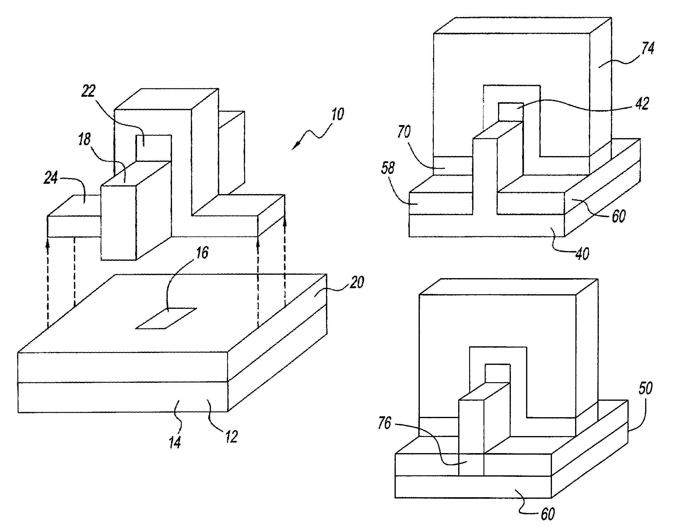
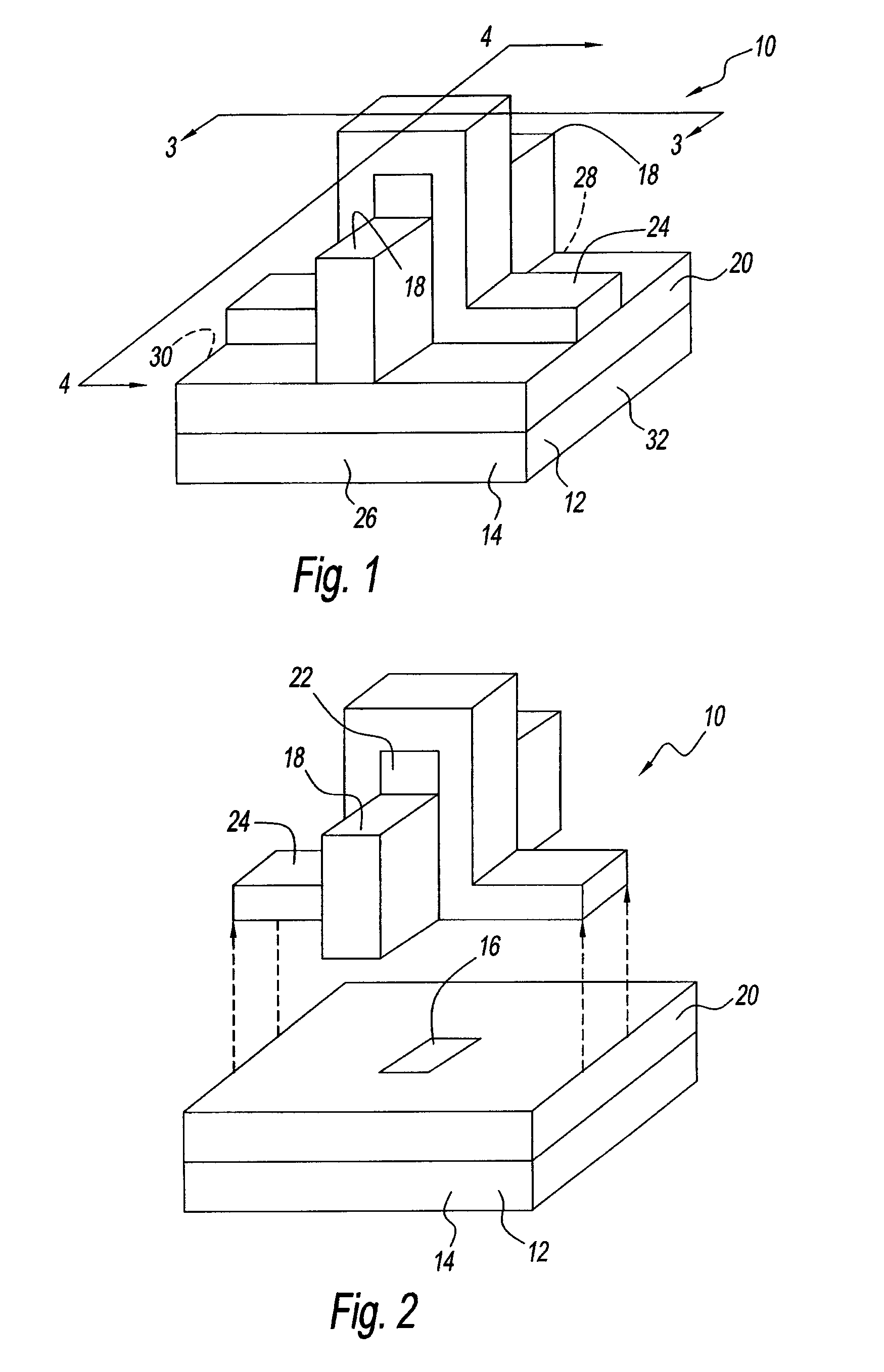
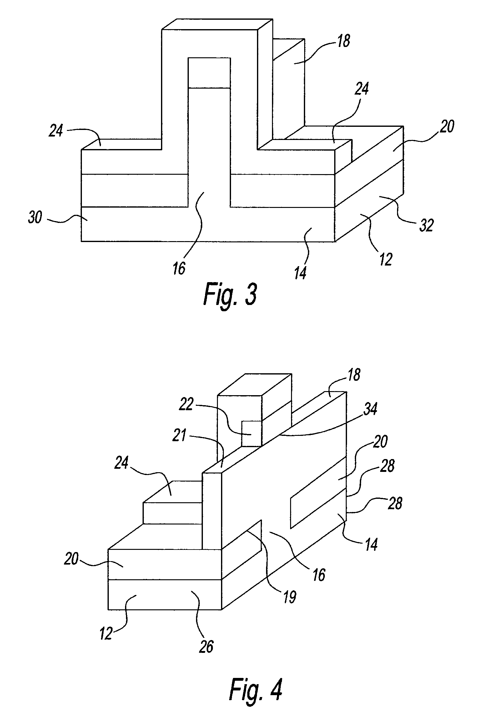
[0024]The device of the present invention is substantially free of the floating body problem found in prior art FinFET devices. The device of the present invention provides body contact that is aligned with the FinFET channel region while providing for isolation between individual fins and between FinFET junctions and the substrate. This body contact can be characterized as “self-aligning” because no positioning is required between the fin, gate, and substrate. The self-aligning body contact is formed via selective oxygen implantation that is masked at the intersection of the fin and the gate.

[0025]An embodiment of the FinFET device of the present invention is shown, for example, in FIGS. 1 to 4, and is generally referenced by the numeral 10. Device 10 has a silicone substrate 12 defining a planar body 14, a medial body 16, and a fin 18. Silicone substrate 12 is unitary with planar body 14, medial body 16, and fin 18 being integrally connected. Device 10 also has a first oxide layer...


PUM


Abstract

There is a FinFET device. The device has a silicon substrate, an oxide layer, and a polysilicone gate. The silicon substrate defines a planar body, a medial body, and a fin. The planar body, the medial body, and the fin are integrally connected. The medial body connects the planar body and the fin. The planar body extends generally around the medial body. The fin is situated to extend substantially from a first side of the substrate to an opposing second side of the substrate. The fin is substantially perpendicularly disposed with respect to the planar body. The first oxide layer is situated on the planar body between the planar body and the fin. The oxide layer extends substantially around the medial body. The polysilicone gate is situated on the oxide layer to extend substantially from a third side to an opposing fourth side of the substrate. The gate is situated to extend across the fin proximal to a medial portion of an upper surface of the fin. There is also a process for making a FinFET device.

Description

BACKGROUND OF THE INVENTION[0001]1. Field of the Invention[0002]The present invention relates to a FinFET device. The present invention further relates to a process for making a FinFET device.[0003]2. Description of the Related Art[0004]FinFET transistors are candidates for next generation CMOS technologies. Conventional FinFET devices typically have an SOI substrate, a fin, and a gate with an oxide layer between the substrate and the fin. Such conventional devices lack body connection between the substrate and the fin, which causes difficulties in controlling floating body voltage.[0005]A FinFET device proposed in the art for addressing floating body voltage difficulties employs a body connection between the substrate and the fin along the entire length of the fin. While the floating body voltage difficulty is addressed, undesirable levels of current leakage occur in the regions of the fin outside the gate.[0006]It would be desirable to have a FinFET device that is substantially fr...

Claims


Application Information

Patent Timeline
Patent Type & Authority Patents(United States)
IPC IPC(8): H01L21/336
CPCH01L29/66795H01L29/785
Inventor DYER, THOMAS W.YANG, HAINING S.
Owner GLOBALFOUNDRIES INC
Why Eureka
Try Eureka