Programmable microtransformer

a microtransformer and programming technology, applied in the field of microtransformers, can solve the problems of increasing the mass, volume and cost of the transformer, traditional fabrication methods precluding the use of common transformers as embedded systems, and the foregoing examples simply cannot be built effectively using printed circuit board fabrication

Inactive Publication Date: 2008-11-25
THE UNITED STATES OF AMERICA AS REPRESENTED BY THE SECRETARY OF THE NAVY
View PDF15 Cites 24 Cited by
  • Summary
  • Abstract
  • Description
  • Claims
  • Application Information

AI Technical Summary

Benefits of technology

[0017]It is another aspect to reduce or eliminate magnetic core materials in miniature transformers.
[0020]These and other aspects are accomplished by a programmable microtransformer with windings embedded in a thin film substrate. The windings are flat wire traces embedded into the substrate, primary on one side and secondary on the other. The secondary windings may be planar or different coils spatially arrayed throughout the thickness of the substrate. Upon energizing the primary the resulting magnetic flux penetrates the substrate. The secondary has multiple tap points, effectively providing multiple secondary coils referenced to the single primary coil. Each tap point is bridged to a field effect or CMOS transistor path by which digital controls permit dynamic adjustment of the turns ratio. The final secondary output depends on which transistor paths are activated. Unlike conventional wound component transformers, it becomes possible to have multiple secondary outputs from a single secondary coil, and a digitally programmable turns ratio. Moreover, the microtransformer layout is scalable based on the relative size of the circuit card on which it resides. Thus, the transformer design is well suited for a MEMs based implementation.

Problems solved by technology

Most transformers are manufactured using an iron-based core material wrapped with wire windings, but this configuration increases their mass, volume and cost.
Traditional fabrication methods preclude the use of common transformers as embedded systems (part of a larger overall system or product) because space confines require more versatile components.
Indeed, some of the foregoing examples simply cannot be built effectively using printed circuit board fabrication techniques because they require vertical angled traces (connecting layer-to-layer), and cannot be done without drilling a hole through the board.
The existing microtransformers have a second limitation in that their turns ratios are typically fixed, and it is difficult to dynamically configure and control the turns ratio.

Method used


Image

  • Programmable microtransformer
  • Programmable microtransformer
  • Programmable microtransformer

Examples


Embodiment Construction

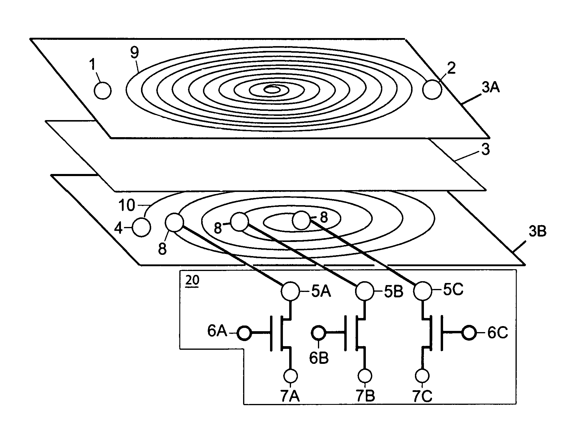
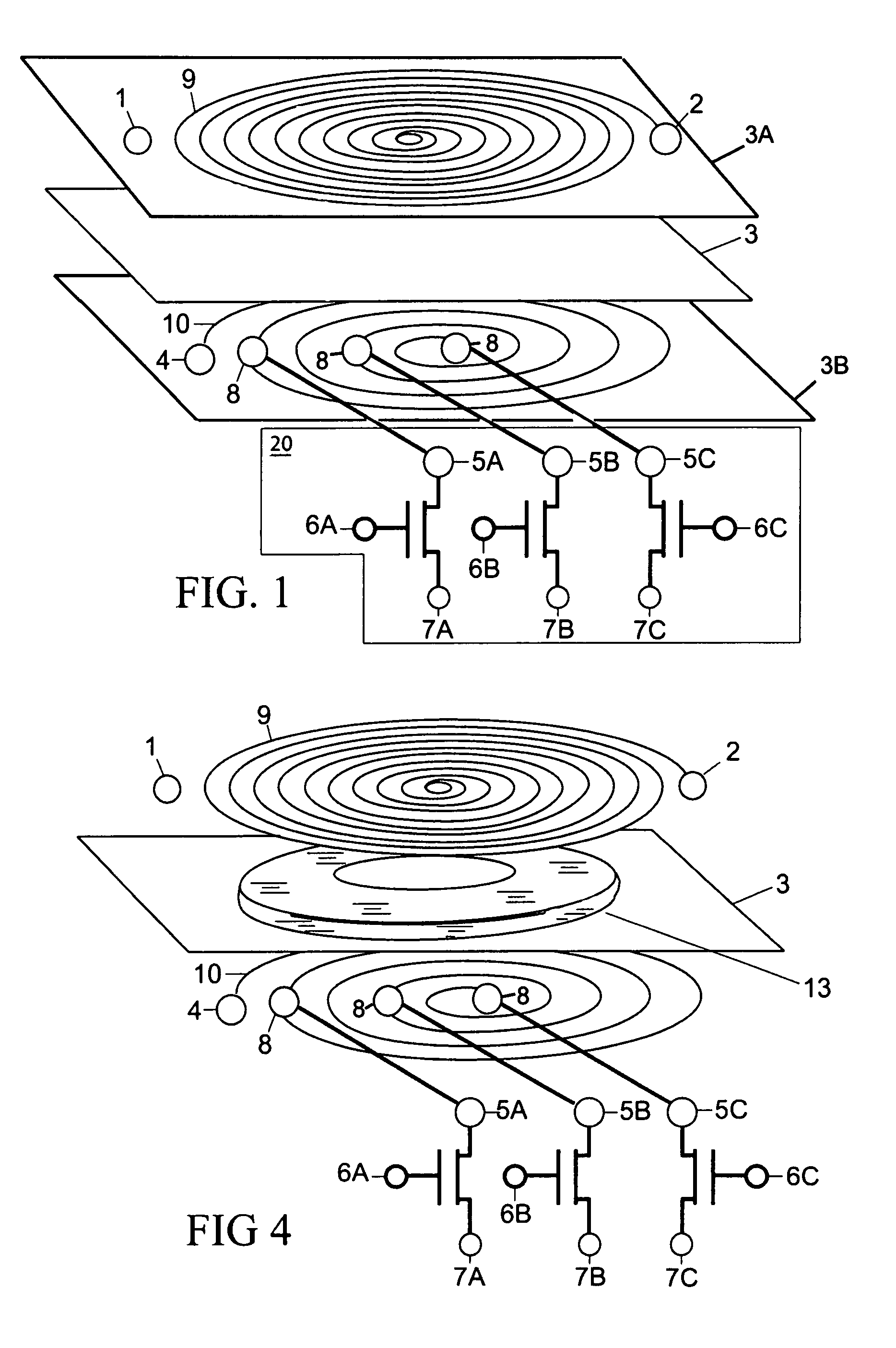
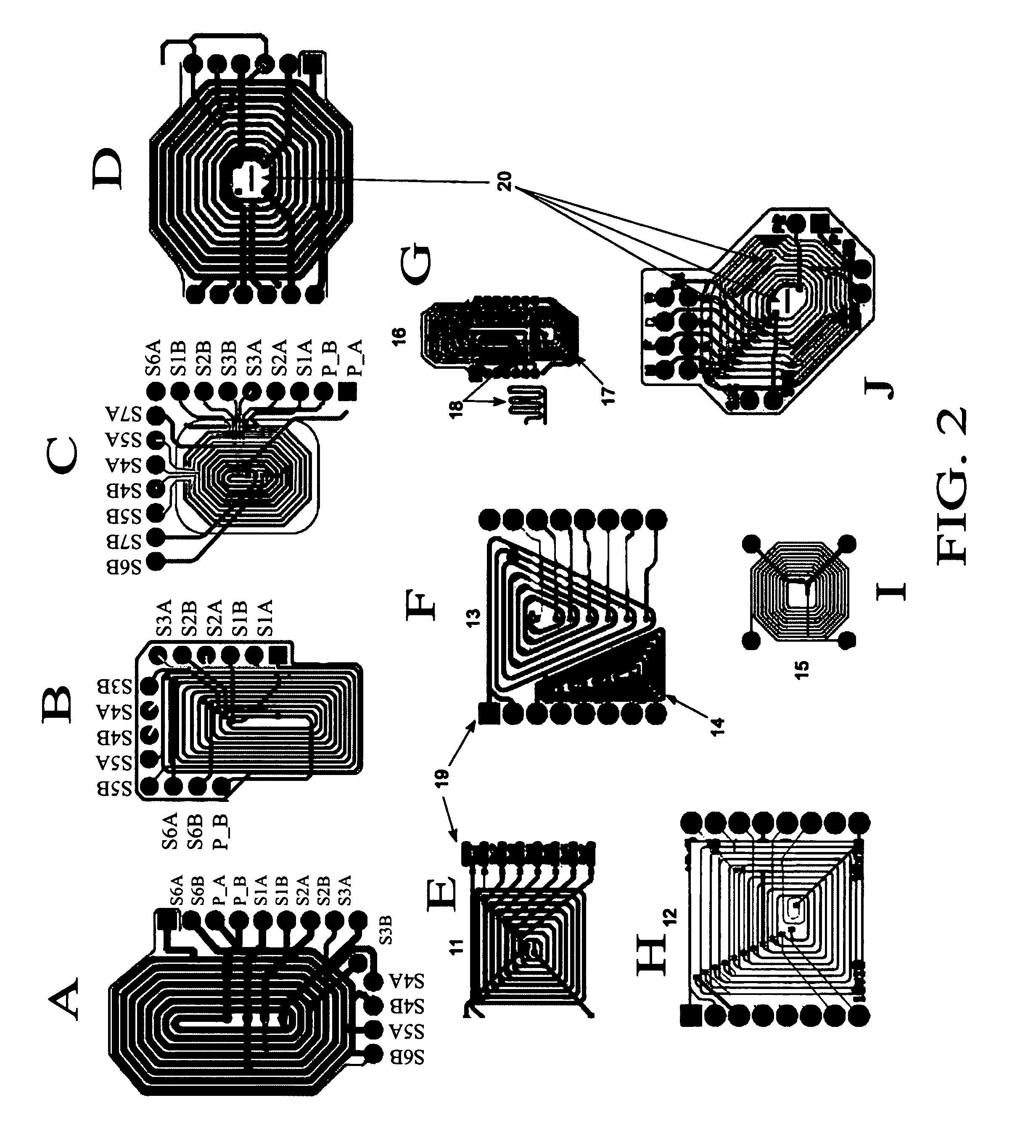
[0029]An exemplary embodiment of the invention is a programmable microtransformer design incorporating flat-wire windings embedded in a thin-film substrate, the secondary windings having multiple tap points connected to digital controls that permit dynamic adjustment of the turns ratio. A method of production is also disclosed.

[0030]FIG. 1 illustrates a basic embodiment of a transformer 2 according to the present invention with both of two windings 9, 10, where each is partially, or completely, initially embedded into a substrate 3A and a substrate 3B, respectively. Substrates 3A and 3B are merged or sandwiched to form a single layer substrate 3 so that windings 9 and 10 are respectively, partially or completely, embedded into the single layer substrate 3. This embodiment is constructed with a flat wire trace as the primary winding 9. Primary winding 9, and its input leads 1, 2, are embedded into substrate 3 on one side, and secondary winding 10 is embedded on the other side. In ope...


PUM

PropertyMeasurementUnit
diameteraaaaaaaaaa
frequenciesaaaaaaaaaa
thicknessaaaaaaaaaa

Abstract

A programmable transformer incorporating windings embedded in a thin film substrate. The windings are flat wire traces embedded into the substrate, primary on one side and secondary on the other. The secondary windings may be planar or different coils spatially arrayed throughout a thickness of the substrate. The secondary winding may include multiple tap points, effectively providing multiple secondary coils referenced to the single primary coil. Each tap point is bridged to a field effect or CMOS transistor path by which a digital controls permit dynamic adjustment of the turns ratio. The final secondary output depends on the activated transistor paths. Multiple secondary outputs from a single secondary coil and a digitally programmable turns ratio are available aspects.

Description

[0001]The present application is a Continuation Application of prior U.S. patent application Ser. No. 11 / 650,759 filed on Dec. 15, 2006 now U.S. Pat. No. 7,298,238.STATEMENT OF GOVERNMENT INTEREST[0002]The invention described herein may be manufactured and used by or for the Government of the United States of America for governmental purposes without the payment of any royalties thereon or therefore.BACKGROUND OF THE INVENTION[0003]The present invention relates to microtransformers and, more particularly, to a programmable microtransformer design incorporating flat-wire windings embedded in a thin-film substrate, the secondary windings having multiple tap points connected to digital controls that permit dynamic adjustment of the turns ratio. The microtransformer layout is scalable based on the relative size of the circuit card on which it resides.[0004]Electrical transformers are commonly implemented as discrete analog components. Most transformers are manufactured using an iron-bas...

Claims


Application Information

Patent Timeline
Patent Type & Authority Patents(United States)
IPC IPC(8): H01F5/00
CPCH01F21/12H01F27/2804H01F17/0006H01F2021/125H03K17/693
Inventor EATON, DERAN S.DAILY, ROBERT M.
Owner THE UNITED STATES OF AMERICA AS REPRESENTED BY THE SECRETARY OF THE NAVY
Why Eureka
Try Eureka