Collector tailored structures for integration of binary junction transistors

a technology of binary junction transistors and tailored structures, applied in the field of semiconductor devices, can solve the problems of performance tradeoffs, bicmos devices formed without tailoring specific characteristics, etc., and achieve the effect of reducing dopant concentration and facilitating bicmos fabrication

Active Publication Date: 2008-12-09
TEXAS INSTR INC
View PDF9 Cites 0 Cited by
  • Summary
  • Abstract
  • Description
  • Claims
  • Application Information

AI Technical Summary

Benefits of technology

[0006]Aspects of the present invention facilitate BiCMOS device fabrication by permitting the tailoring of bipolar device operational parameters without employing additional implantation and / or other processing. An intrinsic dilute mask is employed for forming a deep well region that yields varied regions of dopant concentration without employing varied implants. The intrinsic dilute mask includes at least a blocking portion that can reduce dopant concentration within an impact ionization region and, therefore increase breakdown voltage. Additionally, the mask can include a non-blocking portion, typically within the blocking portion, that permits higher dopant concentrations, for example, to facilitate drive current and / or device speed.

Problems solved by technology

While such integration does serve to minimize manufacturing costs, in some cases the integration causes performance tradeoffs to be made.
One problem that can result from this integration is forming BiCMOS devices without tailoring specific characteristics, such as breakdown voltage due to the integration.
As a result, the devices are formed with operational and / or performance characteristics that cannot be tailored.

Method used


Image

  • Collector tailored structures for integration of binary junction transistors
  • Collector tailored structures for integration of binary junction transistors
  • Collector tailored structures for integration of binary junction transistors

Examples


Embodiment Construction

[0022]One or more aspects of the present invention are described with reference to the drawings, wherein like reference numerals are generally utilized to refer to like elements throughout, and wherein the various structures are not necessarily drawn to scale. In the following description, for purposes of explanation, numerous specific details are set forth in order to provide a thorough understanding of one or more aspects of the present invention. It may be evident, however, to one skilled in the art that one or more aspects of the present invention may be practiced with a lesser degree of these specific details. In other instances, known structures and devices are shown in block diagram form in order to facilitate describing one or more aspects of the present invention.

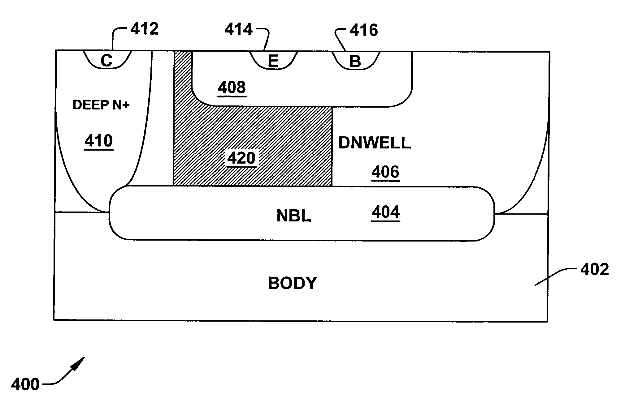
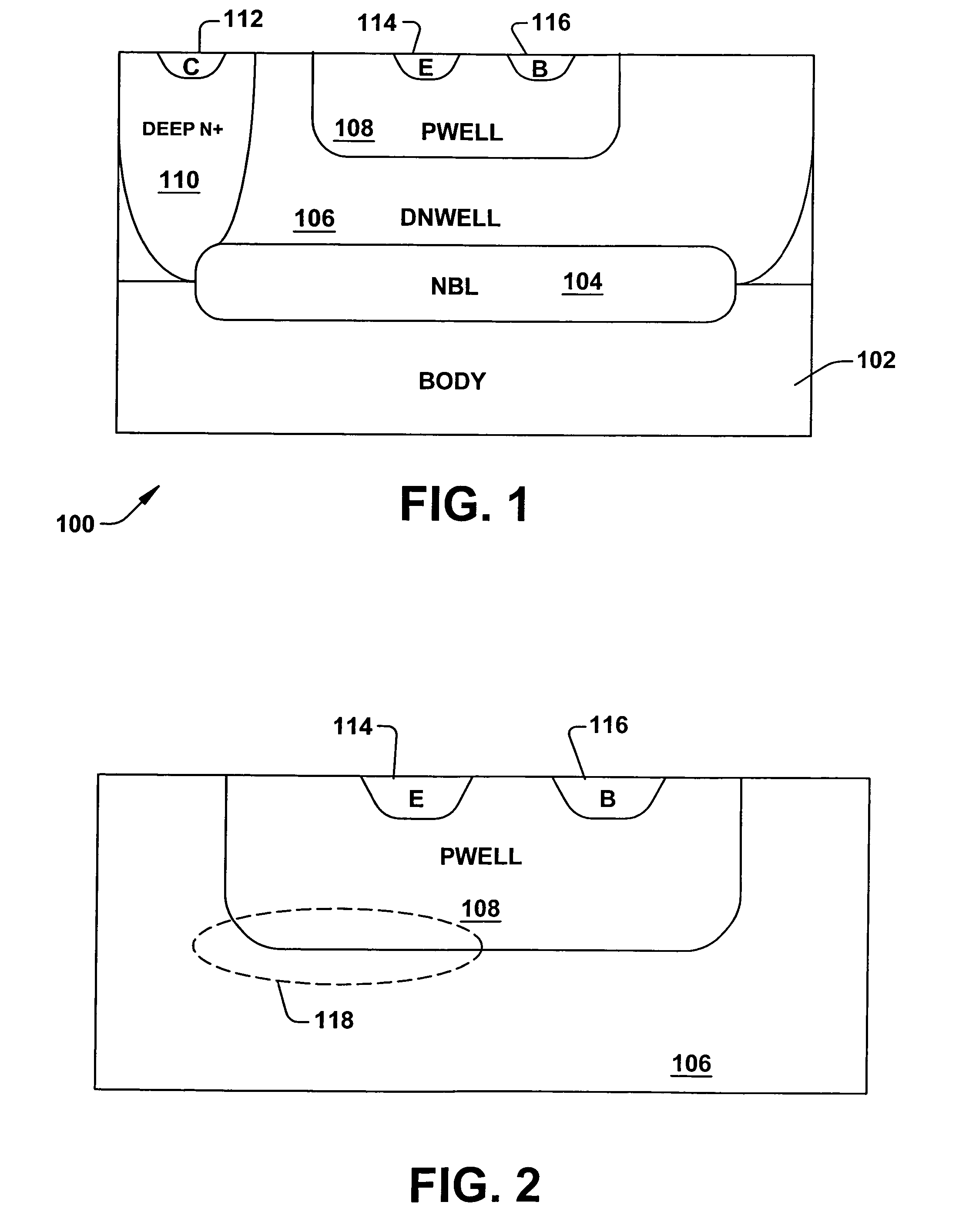
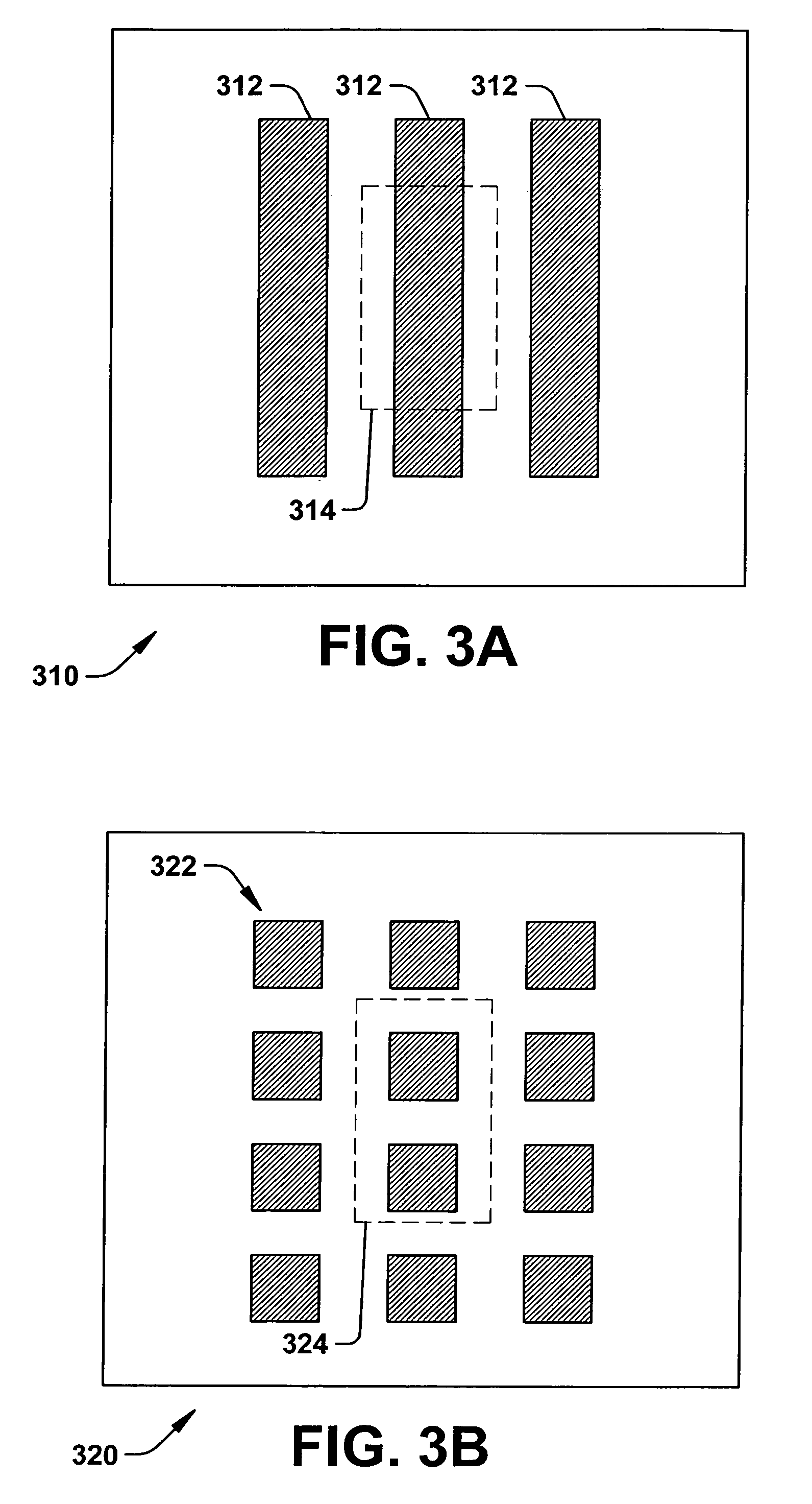
[0023]Aspects of the present invention facilitate BiCMOS fabrication by tailoring dopant profiles within regions of bipolar devices. An intrinsic dilute mask is employed to selectively alter the dopant profile of s...


PUM


Abstract

A bipolar transistor is formed in an integrated BiCMOS process. A buried layer is formed in a semiconductor body. An intrinsic dilute mask is formed over the buried layer that covers at least a portion of a selected region of a target deep well region. The intrinsic dilute mask is employed to implant a dopant into the target deep well region to form a deep well region with the selected region having a lowered dopant concentration. The lowered dopant concentration can yield a higher breakdown voltage for the bipolar device. The intrinsic dilute mask mitigates implantation within the selected region.

Description

FIELD OF INVENTION[0001]The present invention relates generally to semiconductor devices and more particularly relates to methods of adjusting dopant profiles within the intrinsic region to tailor device characteristics.BACKGROUND OF THE INVENTION[0002]Complementary metal oxide semiconductor (CMOS) is an integrated circuit technology offering low power consumption, ease of circuit design, and increasingly high performance with device scaling. Bipolar complementary metal oxide semiconductor (BiCMOS) is an integrated circuit technology that combines bipolar devices with CMOS to yield integrated circuit devices that can have reduced noise, improved linearity, device matching, and high drive capacity, and permit improved performance. BiCMOS integrated circuits have bipolar and MOS transistors formed on the same semiconductor body or substrate. One significant advantage of such devices is that they combine the high power and fast switching speeds of bipolar devices with the high density ...

Claims


Application Information

Patent Timeline
Patent Type & Authority Patents(United States)
IPC IPC(8): H01L21/331H01L21/8222
CPCH01L21/8249H01L29/0821H01L29/6625H01L29/66272
Inventor CHUANG, MING-YEHSWANSON, LELAND S.
Owner TEXAS INSTR INC
Why Eureka
Try Eureka