Three-dimensional multichip module

a multi-chip module and three-dimensional technology, applied in the direction of electrical equipment, semiconductor devices, semiconductor/solid-state device details, etc., can solve the problems of inconvenient multi-chip structure, adjacent chips may overheat, and conventional multi-chip structure has limited space available on the side of the structure for interconnection wiring, etc., to achieve the effect of reducing the space occupied by the chips inside the system, improving cooling, and high heat per unit area

Inactive Publication Date: 2008-12-16
MICRON TECH INC
View PDF82 Cites 22 Cited by
  • Summary
  • Abstract
  • Description
  • Claims
  • Application Information

AI Technical Summary

Benefits of technology

[0018]Advantageously, the present invention provides densely packaged multichip structures that incorporates memory and non-memory chips in the same module. As such, chips of an entire system can be placed in the module so as to reduce the space occupied by the chips inside the system. Furthermore, the chips that generate high heat per unit area or require extensive interconnection with other chips in the module are positioned on the lateral faces of the base structure in a manner such that the outer surface of the chip is not in contact with other chips so as to permit improved cooling and more efficient wiring. These and other advantages of the present invention will become more fully apparent from the following description taken in conjunction with the accompanying drawings.

Problems solved by technology

Disadvantageously, these multichip structures may not be suitable for IC chips that generate excessive heat during operation because it is difficult for heat to dissipate when the chips are sandwiched in a stack with other chips.
Moreover, chips that generate excessive heat can transfer heat to adjacent chips in the stack and cause the adjacent chips to also overheat.
Furthermore, the conventional multichip structures have limited space available on the side of the structure for interconnection wiring.
As such, these structures may also not be suitable for chips that require numerous electrical connections to other chips in the same stack.
Conversely, non-memory chips such as processor chips, logic chips, and A to D converter chips are usually not included as part of a multichip module because these chips generate higher heat per unit area and can be difficult to cool when sandwiched in a stack with other chips.
In addition to cooling problems, processor chips, in particular, often require extensive interconnection with other chips in the module.
In some instances, there is insufficient space on the multichip structure to accommodate all the necessary conductive leads required to interconnect the processor chips to various other chips in the module.
Although through chip connections have been proposed to make inter-chip connections, see for example, U.S. Pat. No. 5,270,261, the process of forming these connections adds to the cost and complexity of fabrication.

Method used


Image

  • Three-dimensional multichip module
  • Three-dimensional multichip module
  • Three-dimensional multichip module

Examples


Embodiment Construction

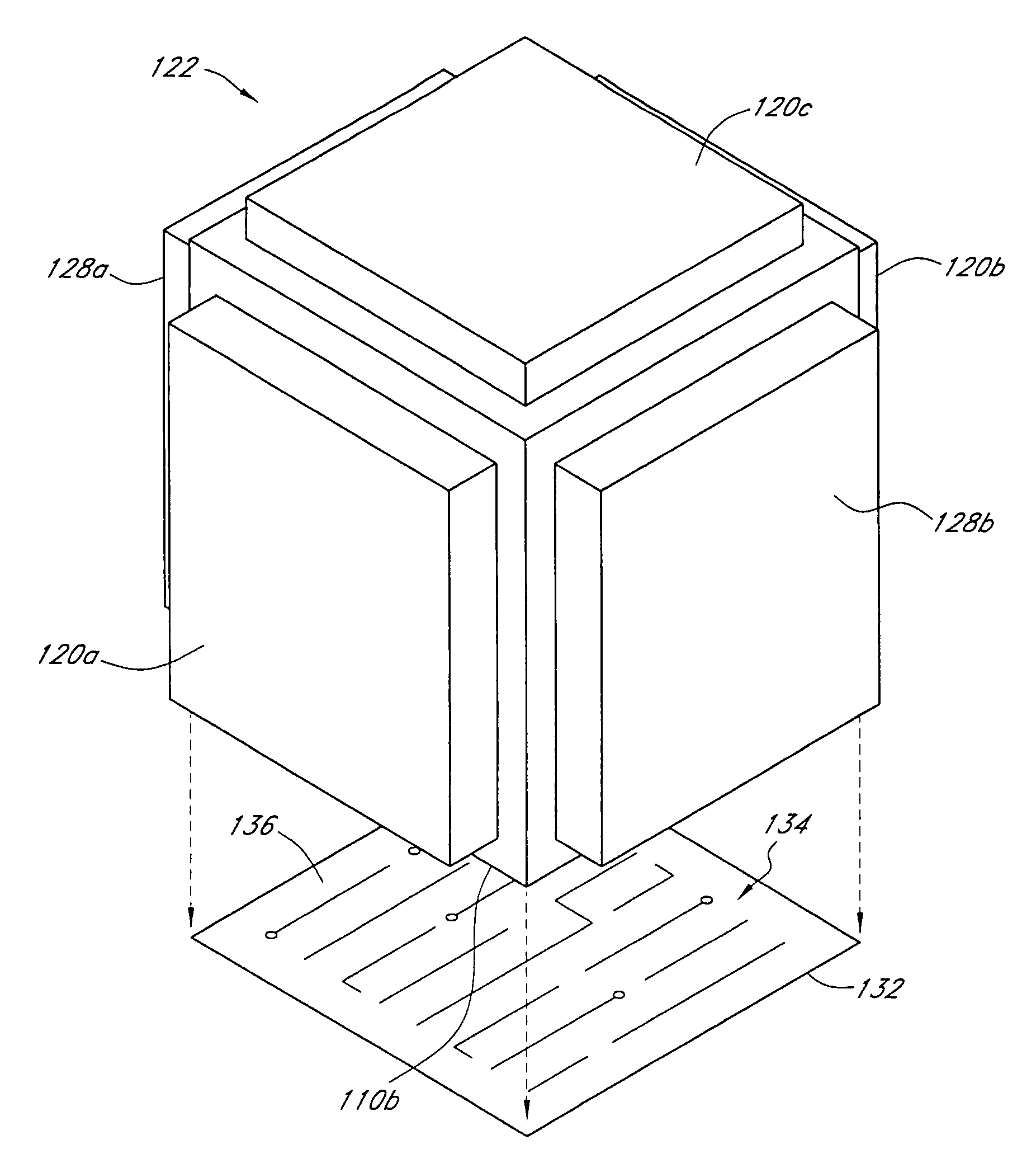
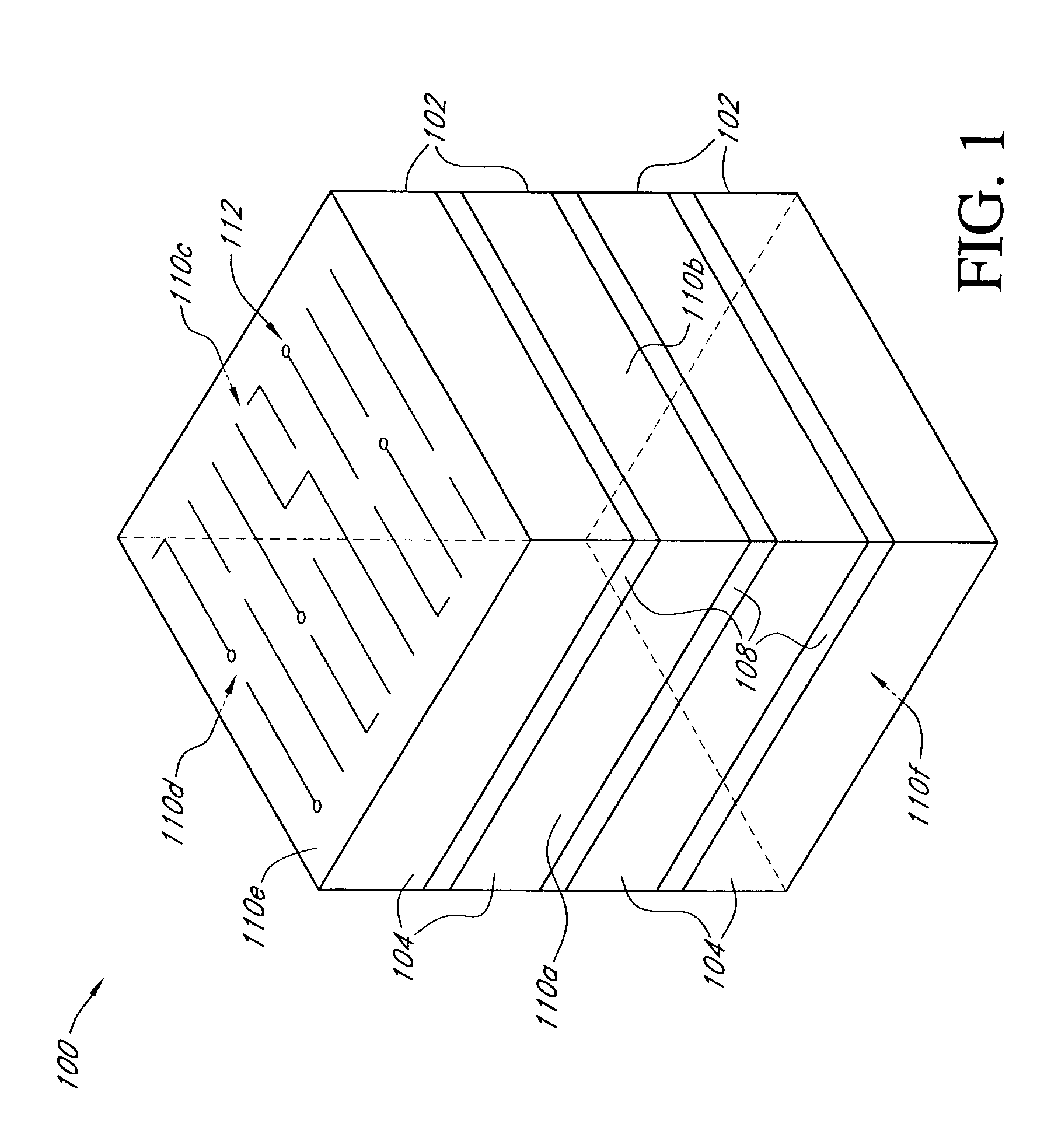
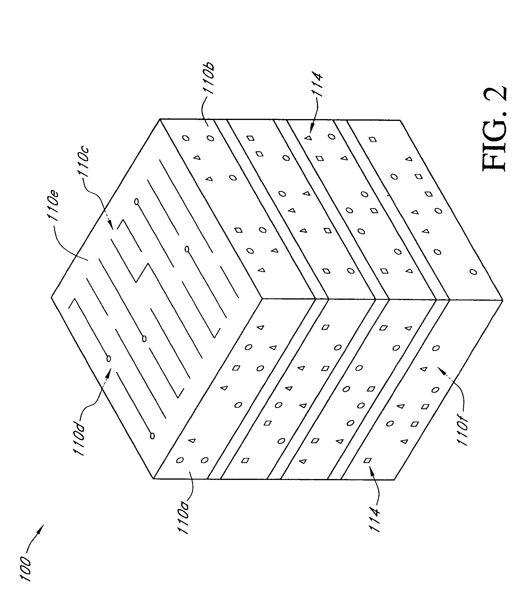
[0024]References will now be made to the drawings wherein like numerals refer to like parts throughout. FIG. 1 provides a general perspective view of a base structure 100 of a multichip module of the preferred embodiment. As FIG. 1 shows, the base structure 100 comprises a plurality of integrated circuit chips 102 stacked and secured together in a known manner to form a three-dimensional rectangular structure. Each chip 102 comprises a semiconductor substrate 104 such as a silicon substrate, that carries a variety of integrated devices and circuitry formed using conventional semiconductor manufacturing processes. Furthermore, it is generally understood that each chip 102 in the stack has conductive leads that extend to one edge of the chip so as to provide electrical contact with external circuitry.

[0025]As shown in FIG. 1, the base structure 100 has four lateral faces 110a, b, c, d that are defined by the side surfaces of the chips 102. Preferably, the first lateral face 110a is su...


PUM


Abstract

A three-dimensional multichip module having a base structure formed by a plurality of chips secured together in a stack and a plurality of exterior chips mounted to the exterior faces of the base structure. The multichip module may incorporate memory chips, processor chips, logic chips, A to D converter chips, and other chips in a compact package. The module permits chips that require extensive cooling to be positioned within the structure in a manner such that a large surface area of the chip is not in contact with other chips. The module also permits extensive interconnection between chips within the module.

Description

RELATED APPLICATIONS[0001]This application is a continuation application of U.S. patent application Ser. No. 10 / 178,183 filed Jun. 21, 2002 now U.S. Pat. No. 6,790,702 entitled “A THREE-DIMENSIONAL MULTICHIP MODULE”, which claims priority to U.S. Pat. No. 6,433,413 filed Aug. 17, 2001, each is hereby incorporated by reference in its entirety.BACKGROUND OF THE INVENTION[0002]1. Field of the Invention[0003]This invention relates to high density electronic packaging modules, and more particularly, to a three-dimensional multichip module comprised of memory and processor chips packaged in a single compact structure.[0004]2. Description of the Related Art[0005]To provide improved performance, manufacturers of integrated circuit chips continually strive to increase packaging density, which has led to the development of high density electronic packaging modules such as three-dimensional multichip structures. These multichip structures typically include a plurality of semiconductor chips th...

Claims


Application Information

Patent Timeline
Patent Type & Authority Patents(United States)
IPC IPC(8): H01L21/44H01L23/482H01L25/065H01L25/18
CPCH01L23/4822H01L25/065H01L25/0657H01L25/18H01L2225/06513H01L2225/06527H01L2225/06551H01L24/01H01L2924/14H01L2224/32145H01L2924/00
Inventor FARRAR, PAUL A.
Owner MICRON TECH INC
Why Eureka
Try Eureka