This helps you quickly interpret patents by identifying the three key elements:
Problems solved by technology
Method used
Benefits of technology
Benefits of technology
[0015]The present invention provides a light-emitting device providing both luminescence to a top surface and luminescence to a bottom surface with an image display having an uniform color tone and high quality in a light-emitting device (an EL element) where materials of a cathode and an anode are transparent.
[0024]As shown in FIGS. 6A and 6B, in a dual emission (both top and bottom emissions) type light-emitting device, two pieces of polarizing plates are disposed sandwiching a light-emitting panel so that a direction of polarization is to be perpendicular thereto, thereby preventing a display from being hard to be recognized because of transparency to see a background when watched from one side.
Problems solved by technology
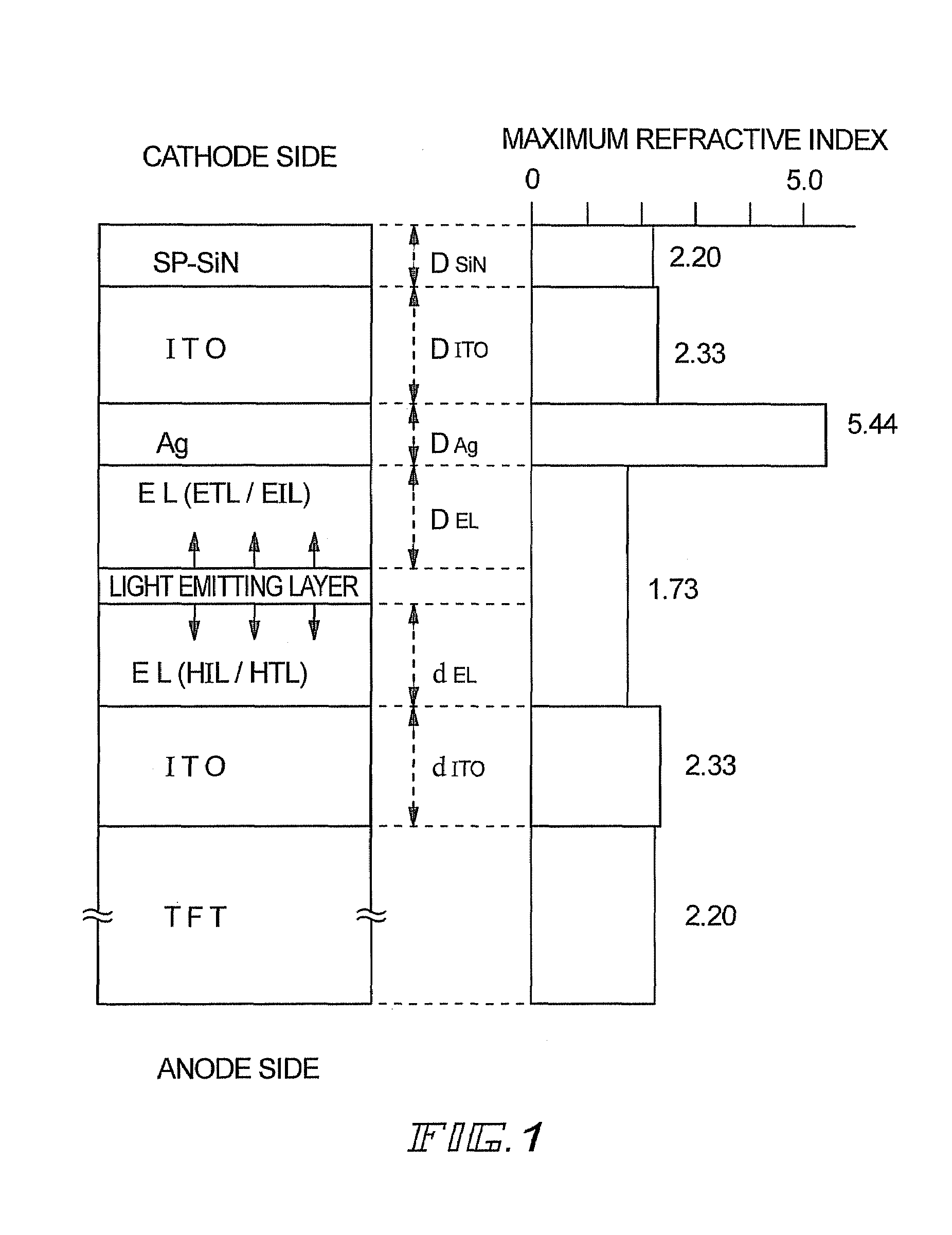
However, the difference in optical characteristics (such as a color tone) between luminescence from a top surface and luminescence from a bottom surface arise for an interference effect by a difference of an optical distance.
When a light-emitting device (an EL device) of three kinds (red, green, and blue) that materials of a cathode and an anode are transparent is used to manufacture a light-emitting display device of full color, problem that a color coordinate is different between luminescence from a top surface and luminescence from the bottom surface arises as shown in FIG. 8.
If a color coordinate is different, the same gradation display in the top surface and the bottom surface is impossible.
Method used
Image
Click on the blue label to locate the original text in one second.
Reading with bidirectional positioning of images and text.
Examples
embodiment 1
[0055]In the present embodiment, a dual emission type light-emitting device is described with reference to FIGS. 4A to 4C.
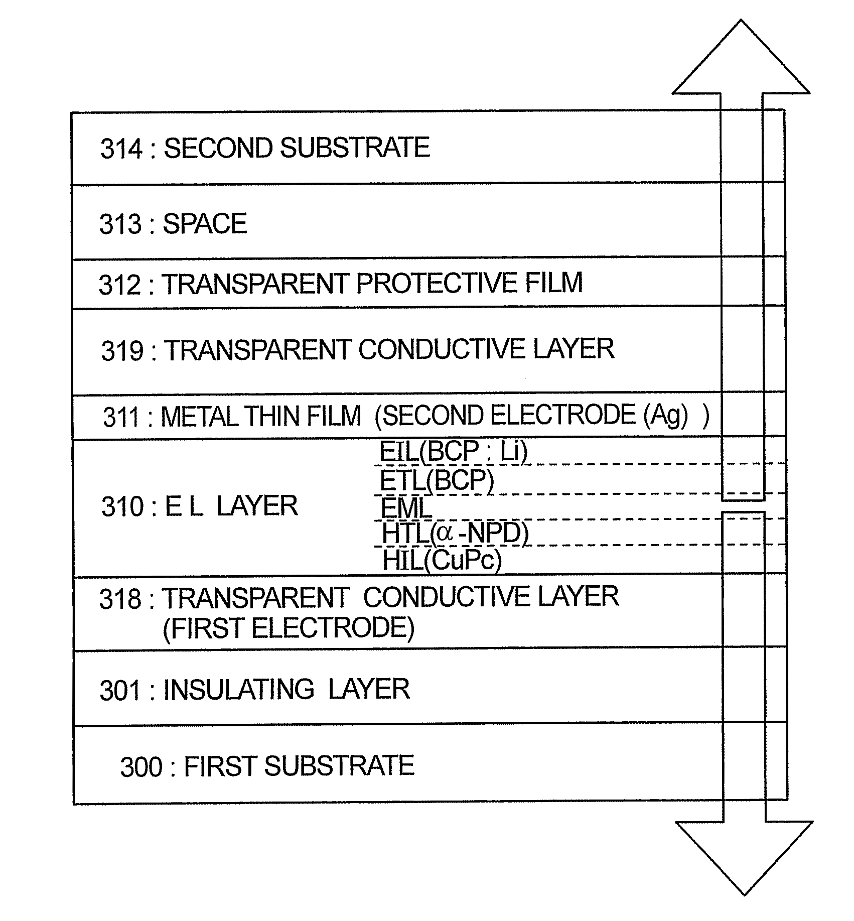
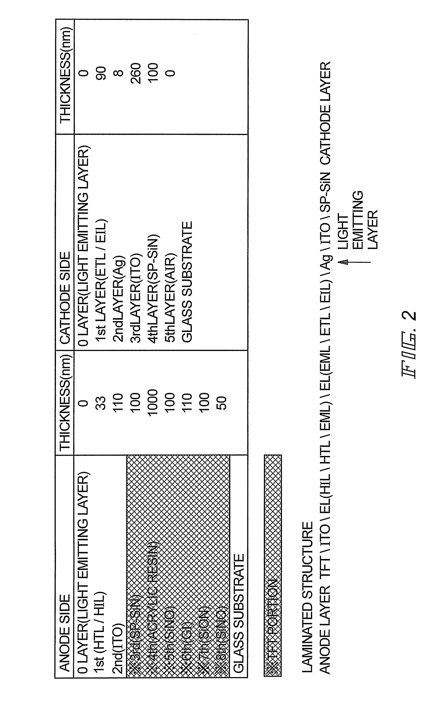
[0056]FIG. 4A is a cross-sectional view of a part of a pixel portion. FIG. 4B shows a simplified view of a laminated structure in a light-emitting region. Luminescence can be emitted to both a top surface and a bottom surface as shown in FIG. 4B. Note that, as for a configuration of a light-emitting region, namely, a configuration of a pixel electrode, a stripe arrangement, a delta arrangement, a mosaic arrangement and the like are mentioned.
[0057]In FIG. 4A, reference numeral 300 denotes a first substrate, 301a and 301b denote insulating layers, 302 denotes a TFT, 318 denotes a first electrode (transparent conductive layer), 309 denotes an insulator (referred to as a partition, a mound), 310 denotes an EL layer, 311 denotes a second electrode, 319 denotes a transparent conductive layer, 312 denotes a transparent protective layer, 313 denotes a space, and 314 den...
embodiment 2
[0075]According to the present embodiment, an example of a portable electronic appliance comprising equal to or more than two display devices is described. FIG. 5A is a side view, and FIG. 5B is a perspective view. A mobile phone shown in FIGS. 5A and 5B comprises a first display device 401 of high quality mainly displaying a color pictorial image and a second display device 402 mainly displaying characters and symbols.
[0076]As shown in FIGS. 5A and 5B, the portable electronic appliance may be one in which a first display device 401 and a second display device 402 are attached each other so as to allow opening and closing freely and so as to sandwich a third display device 403. The third display device 403 can display on both sides. The third display device 403 of a dual emission type can be provided according to the embodiment 1.
[0077]An electronic appliance shown in FIGS. 5A and 5B is a portable electronic appliance in which a cover member having the first display device for displ...
embodiment 3
[0083]According to the present embodiment, an example using an optical film so as not to be transparent to see a background therethrough is shown in FIG. 6 as for a dual emission panel.
[0084]FIG. 6A shows a cross-sectional view of a light-emitting device, and FIG. 6B shows a perspective view thereof. A light-emitting panel 1801 is sandwiched between polarizing plates 1802 and 1803 so as to prevent outside light from passing. The two pieces of polarizing plates can cut off outside light by being disposed perpendicular to a direction of polarization. Light from a light-emitting panel 1801 can perform a display because it passes only one piece of polarizing plates.
[0085]In this way, a light-emitting panel except a light-emitting portion to perform a display becomes black not to be transparent to see a background, even if the display is watched from either side.
[0086]In FIGS. 6A and 6B, the polarizing plates 1802 and 1803 are disposed so as to have a space with the light-emitting panel ...
PUM
Abstract
When materials of a cathode and an anode are transparent and a substrate with transparency is used for a substrate and a sealing substrate, luminescence from a layer including an organic compound can simultaneously perform two ways of display: luminescence passing a cathode and luminescence transmitted in an anode. However, interference effect by an optical distance difference results in difference in optical characteristics (such as a color tone) between luminescence from a top surface and luminescence from a bottom surface. According to the present invention, a light-emitting device having luminescence from a top surface and luminescence from a bottom surface provides both luminescence to a top surface and luminescence to a bottom surface with an image display having an uniform color tone and of high quality by regulating a film thickness of a transparent conductive film disposed on a cathode side and a film thickness of a cathode.
Description
BACKGROUND OF THE INVENTION[0001]1. Field of the Invention[0002]The present invention relates to a light-emitting device with the use of a light-emitting element in which a film including an organic compound (hereinafter, referred to as an “organic compound layer”) disposed between a pair of electrode is provided fluorescence or phosphorescence by applying an electric field, and a method for manufacturing the light-emitting device. A light-emitting device in the present specification may include an image display device, a light-emitting device, or a light source (including a lighting system). In addition, a module that a connector, for example, a FPC (Flexible Printed Circuit), a TAB (Tape Automated Bonding) tape, or a TCP (Tape Carrier Package) is installed in the light-emitting device, a module that a printed wiring board is provided at an end of a TAB tape and a TCP, and a module that an IC (integrated circuit) is mounted directly in the light-emitting device by a COG (Chip On Gl...
Claims
Application Information
Patent Timeline
Application Date:The date an application was filed.
Publication Date:The date a patent or application was officially published.
First Publication Date:The earliest publication date of a patent with the same application number.
Issue Date:Publication date of the patent grant document.
PCT Entry Date:The Entry date of PCT National Phase.
Estimated Expiry Date:The statutory expiry date of a patent right according to the Patent Law, and it is the longest term of protection that the patent right can achieve without the termination of the patent right due to other reasons(Term extension factor has been taken into account ).
Invalid Date:Actual expiry date is based on effective date or publication date of legal transaction data of invalid patent.

