Photo-detection device

a detection device and photo-detection technology, applied in the direction of radiation controlled devices, optical radiation measurement, semiconductor/solid-state device details, etc., can solve the problems of path exhibiting a large parasitic capacitance and failing to detect light accurately

Inactive Publication Date: 2008-12-30
HAMAMATSU PHOTONICS KK
View PDF18 Cites 60 Cited by
  • Summary
  • Abstract
  • Description
  • Claims
  • Application Information

AI Technical Summary

Benefits of technology

[0005]In order to overcome the above-mentioned problems, it is an object of the present invention to provide a photo-detecting apparatus having a structure which can accurately detect light by restraining noises from occurring.
[0007]Since the third substrate, including a common wire for connecting the photodetector devices to the signal processing part, is disposed between the first and second substrates, the photo-detecting apparatus according to the present invention can effectively reduce the length of wiring on the first or second substrate. Preferably, in this case, the photodetector devices are electrically connected to the common wire by way of a first bump disposed between the first and third substrates, whereas the signal processing part is electrically connected to the terminal part by way of a second bump disposed between the second and third substrates.
[0011]In the photo-detecting apparatus according to the present invention, it is preferable that the common wire on the first surface of the third substrate includes a plurality of wiring elements arranged at a predetermined interval, whereas the terminal part on the second surface of the third substrate includes a plurality of terminals arranged at an interval narrower than the interval at which the plurality of wiring elements are arranged. Thus narrowing the interval at which the terminals included in the terminal part are arranged can reduce the size of the second substrate itself, thereby making it possible to position the second substrate on the inner side of the outer periphery of the third substrate.

Problems solved by technology

The inventors have studied conventional optical communication systems in detail, and as a result, have found problems as follows.
Therefore, this path exhibits a large parasitic capacitance.
As a consequence, the conventional photo-detecting apparatus incurs a large noise included in the voltage outputted from the integrating circuit, thus failing to detect light accurately.

Method used


Image

  • Photo-detection device
  • Photo-detection device
  • Photo-detection device

Examples


Embodiment Construction

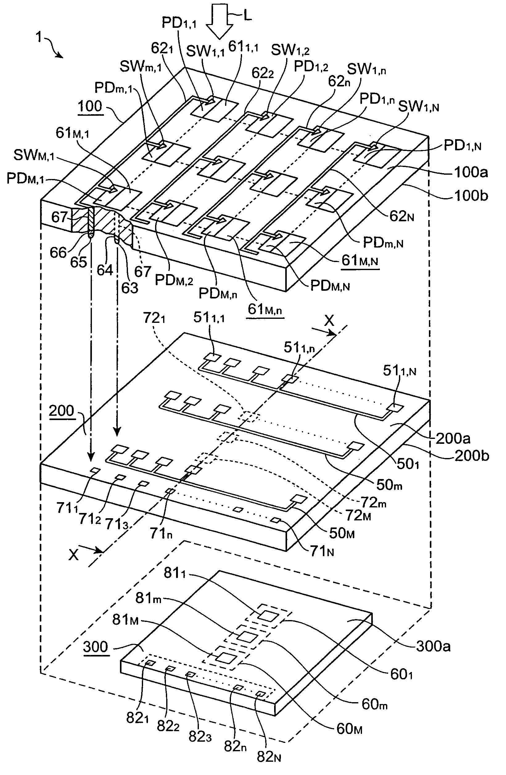
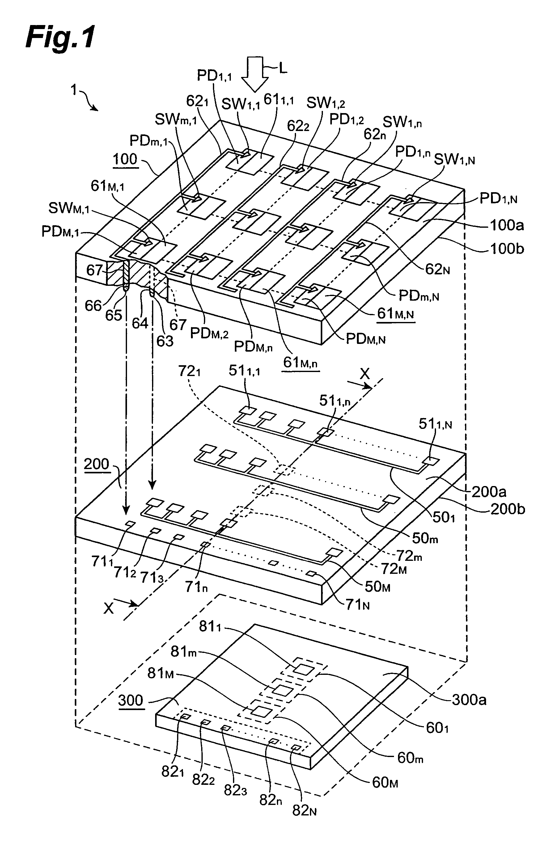
[0027]In the following, embodiments of the photo-detecting apparatus according to the present invention will be explained in detail. with reference to FIGS. 1 to 12. In the explanation of the drawings, constituents identical to each other will be referred to with numerals identical to each other without repeating their overlapping descriptions.

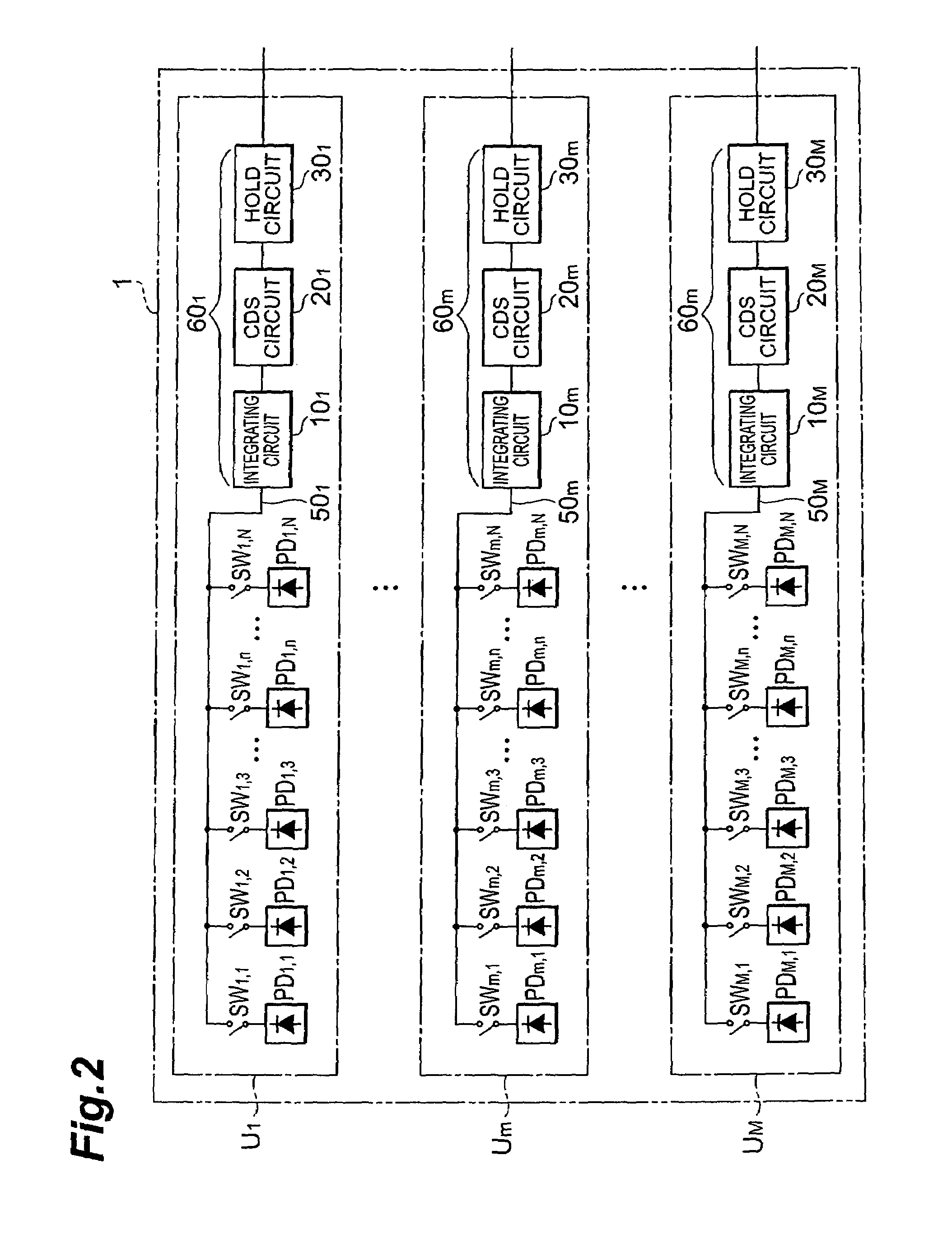
[0028]To begin with, an embodiment of the photo-detecting apparatus according to the present invention will be explained with reference to FIGS. 2 to 4. FIG. 2 is a view showing the configuration of an embodiment of the photo-detecting apparatus according to the present invention. The photo-detecting apparatus 1 shown in FIG. 2 comprises M photo-detecting units (hereinafter referred to as units) U1 to UM. Each unit Um includes N photodiodes PDm,1 to PDm,N, N switches SWm,1 to SWm,N, and a signal processing circuit 60m. Here, M is an integer of at least 1, whereas N is an integer of at least 2. On the other hand, m is an integer of at least 1 b...


PUM


Abstract

The present invention relates to a photo-detecting apparatus having a structure which can accurately detect light by restraining noises from occurring. The photo-detecting apparatus comprises a first substrate having a surface provided with M×N photodiodes and switches; a second substrate having a surface provided with signal processing parts for processing output signals of the photodiodes; and a third substrate arranged between the first and second substrates. The third substrate has a first surface opposing the first substrate and a second surface opposing the second substrate. In the third substrate, M common wires for connecting the photodiodes to the signal processing parts are arranged on the first surface, whereas bonding pads connected to the respective common wires are arranged on the second surface. The photodiodes on the first substrate are electrically connected to their corresponding common wires in the third substrate by way of first bumps, whereas the signal processing parts on the second substrate are electrically connected to their corresponding bonding pads in the third substrate by way of second bumps.

Description

TECHNICAL FIELD[0001]The present invention relates to a photo-detecting apparatus comprising a plurality of photodiodes (photodetector devices) arranged one- or two-dimensionally.BACKGROUND ART[0002]A photo-detecting apparatus is an apparatus comprising a plurality of photodiodes arranged one- or two-dimensionally, and an integrating circuit including an amplifier and a capacitor. In this kind of photo-detecting apparatus, the photodiodes output respective electric charges corresponding to their incident light intensities. The capacitor accumulates thus outputted electric charges, whereas the integrating circuit outputs voltages corresponding to thus accumulated electric charges. In accordance with the output voltages of the integrating circuit, the photo-detecting apparatus detects incident light at photosensitive regions corresponding to positions where the photodiodes are arranged.[0003]Known as an example of this kind of photo-detecting apparatus is one disclosed in Japanese Pat...

Claims


Application Information

Patent Timeline
Patent Type & Authority Patents(United States)
IPC IPC(8): H01L31/00H01L27/146H01L31/02H04N5/374
CPCH01L27/14634H01L27/14636H01L27/14638H01L23/481H01L27/14661H01L2224/0557H01L2924/0002H01L2224/16238H01L2224/05554H01L2224/0401H01L2224/05552G01J1/58
Inventor SUZUKI, YASUHIROMIZUNO, SEIICHIRO
Owner HAMAMATSU PHOTONICS KK
Why Eureka
Try Eureka