AI technical title is built by Patsnap AI team. It summarizes the technical point description of the patent document.
a color imager and filterless technology, applied in the field of imager pixel transistor set, can solve the problem that the wafer bonding process is not a common process in the conventional cmos wafer fabrication facility, and achieve the effect of reducing the area of the imager pixel
Inactive Publication Date: 2008-12-30
SHARP KK
View PDF5 Cites 15 Cited by
Summary
Abstract
Description
Claims
Application Information
AI Technical Summary
This helps you quickly interpret patents by identifying the three key elements:
Problems solved by technology
Method used
Benefits of technology
Benefits of technology
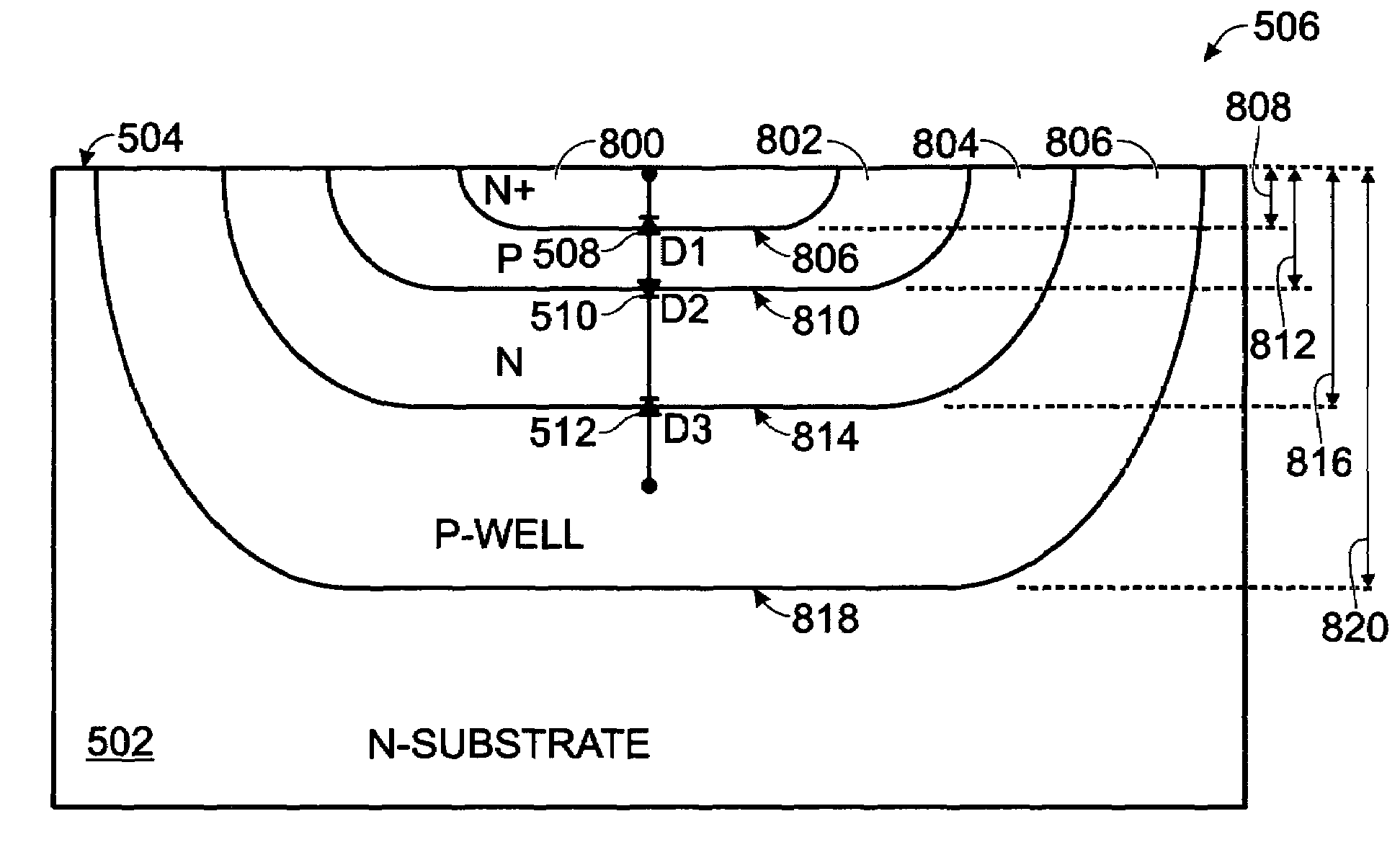
[0017]The present invention describes a filterless triple-junction bulk substrate CMOS color imager with separate blue, green, and red output active pixel sensor circuit signals. There are three (3) junctions in each pixel cell. In one aspect, the layers are N+ / P / N-well / p-substrate. Each photodiode is formed with one junction. The N+ / P junction is blue diode. The P / N-well is green diode, and the N-well / P-substrate junction is the red diode. Therefore, the active photon detection area can be much larger than in previous designs. In addition, the area of the imager pixel can be made much smaller. The active pixel sensing circuit independently reads each individual blue, green, and red diode photovoltaic voltage.
Problems solved by technology
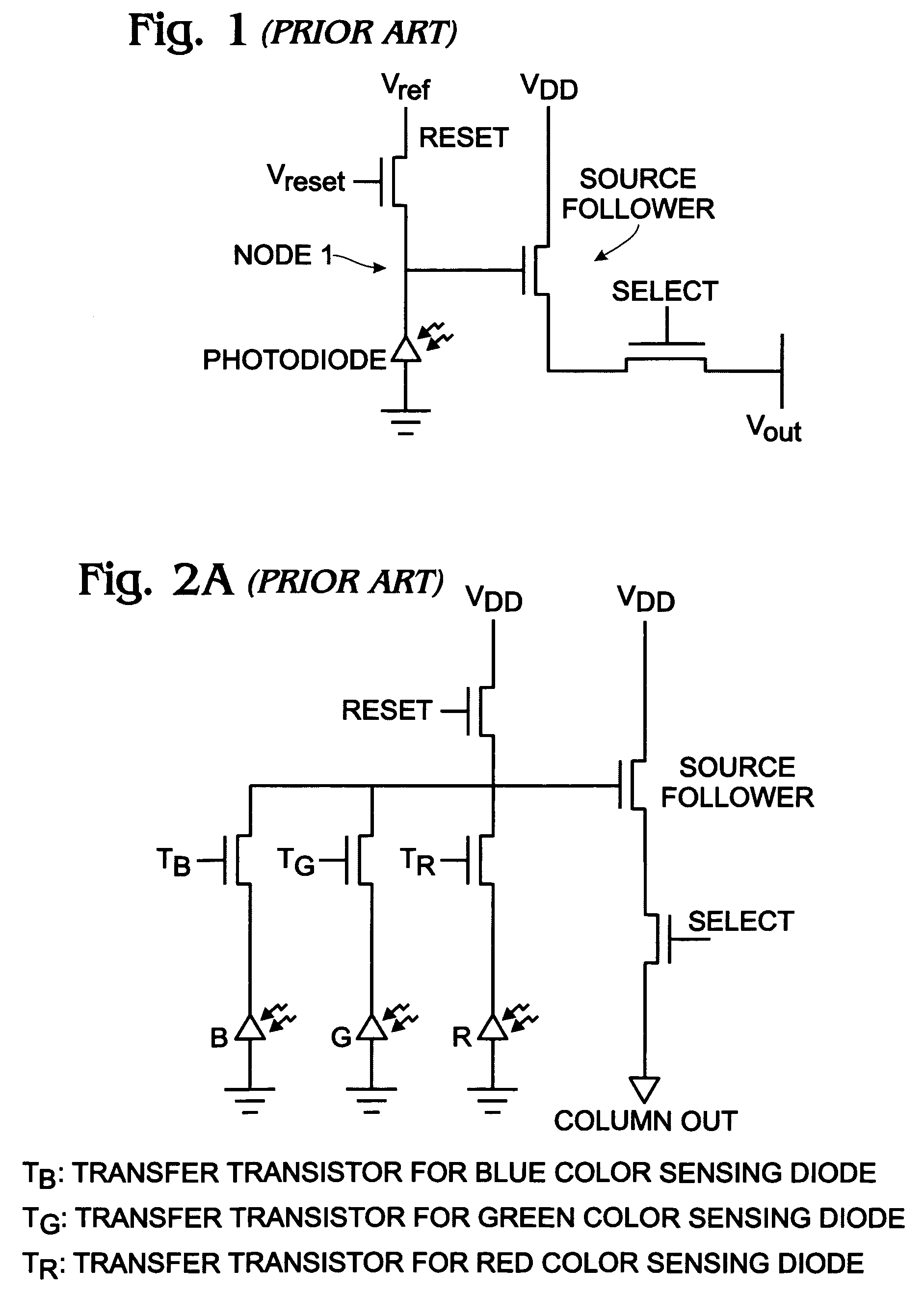
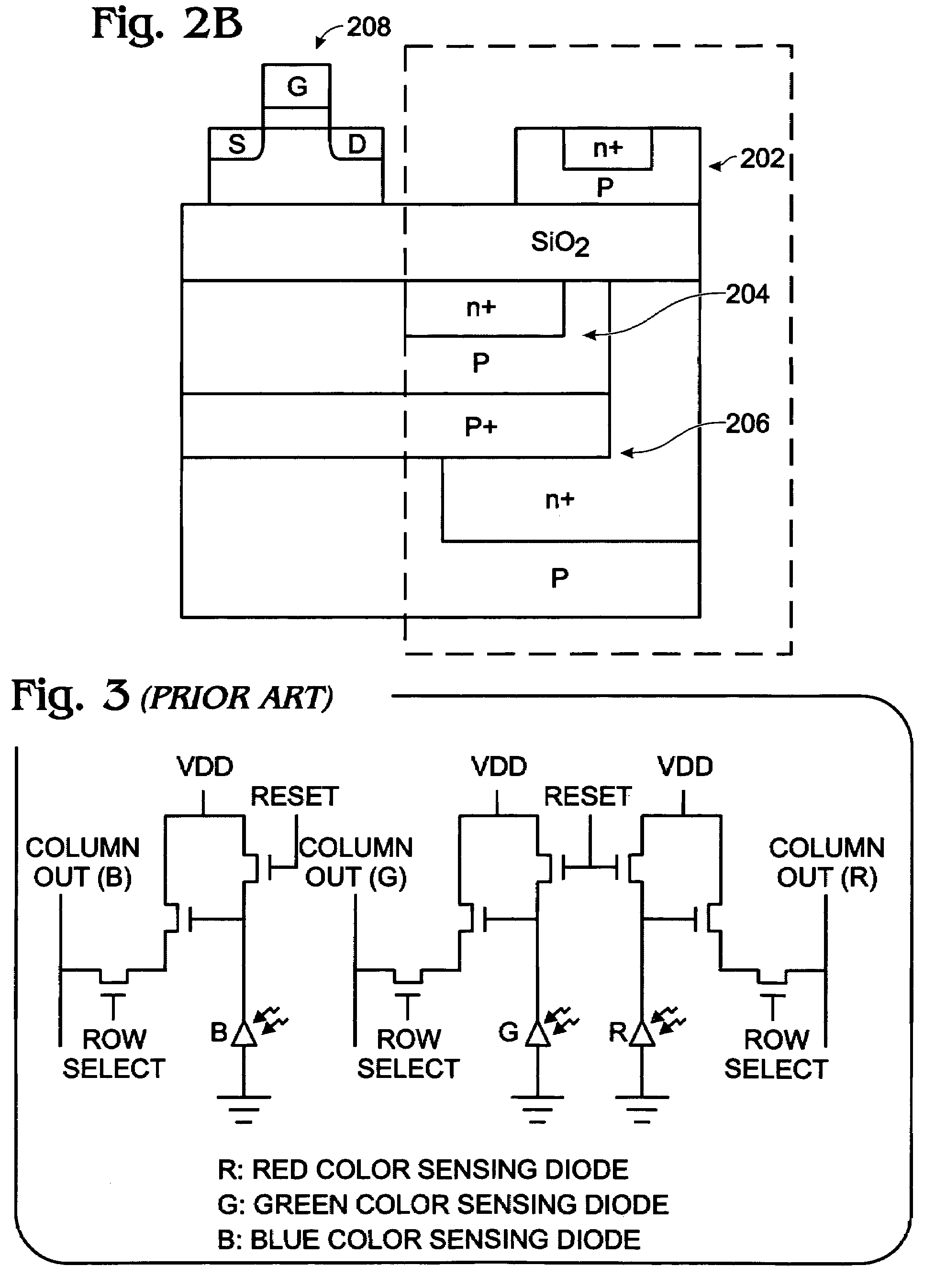
Although the SOI structure is able to reduce the number of junctions required, increase the filling factor, and reduce the pixel size, the wafer bonding process is not a common process in a conventional CMOS wafer fabrication facility.
Method used
Image
Click on the blue label to locate the original text in one second.
Reading with bidirectional positioning of images and text.
Examples
Embodiment Construction
[0042]FIG. 5 is a schematic block diagram depicting a triple-junction complimentary metal-oxide-semiconductor (CMOS) filterless color imager cell. The imager cell 500 comprises a bulk silicon (Si) substrate 502 with a top surface 504. A photodiode set 506, including a first photodiode (D1) 508, second photodiode (D2) 510, and third photodiode (D3) 512, is formed as a triple-junction structure in the Si substrate 502. A transistor set 514 is connected to the photodiode set 506, for detecting an independent output signal for each photodiode.
[0043]More specifically, the transistor set 514 detects an output signal on line 516 for the first photodiode 508, but not the second diode 510 and third photodiode 512, at a first time. The transistor set 514 detects an output signal on line 518 for the second photodiode 510, but not the first diode 508 and third photodiode 512, at a second time. The second time is a different time than the first time. Likewise, the transistor set 514 detects an o...
PUM
Abstract
A triple-junction complimentary metal-oxide-semiconductor (CMOS) filterless color imager cell is provided. The imager cell is made from a bulk silicon (Si) substrate. A photodiode set including a first, second, and third photodiode are formed as a triple-junction structure in the Si substrate. A transistor set is connected to the photodiode set, and detects an independent output signal for each photodiode. Typically, the transistor set is formed in the top surface of the substrate. For example, the Si substrate may be a p-doped Si substrate, and the photodiode triple-junction structure includes the first photodiode forming a pn junction from an n+-doped region at the Si substrate top surface, to an underlying p-doped region. The second photodiode forms a pn junction from the p-doped region to an underlying n-well, and the third photodiode forms a pn junction from the n-well to the underlying p-doped Si substrate.
Description
RELATED APPLICATIONS[0001]This application is a Continuation-in-Part of a patent application entitled, DOUBLE-JUNCTION FILTERLESS CMOS COLOR IMAGER CELL, invented by Hsu et al., Ser. No. 11 / 499,081, filed Aug. 4, 2006 now U.S. Pat. No. 7,233,036,[0002]which is a Continuation-in-Part of a pending patent application entitled, WIDE OUTPUT SWING CMOS IMAGER, invented by Lee et al., Ser. No. 11 / 416,742, filed May 3, 2006,[0003]which is a Continuation-in-Part of a patent application entitled, A REAL-TIME CMOS IMAGER HAVING STACKED PHOTODIODES FABRICATED ON SOI WAFER, invented by Lee et at., Ser. No. 11 / 384,110, filed Mar. 17, 2006 now U.S. Pat. No. 7,419,844. All three of the above-mentioned applications are incorporated herein by reference.BACKGROUND OF THE INVENTION[0004]1. Field of the Invention[0005]This invention generally relates to complementary metal / oxide / semiconductor (CMOS) imaging sensors and, more particularly, to an imager pixel transistor set for reading signals from triple...
Claims
Application Information
Patent Timeline
Application Date:The date an application was filed.
Publication Date:The date a patent or application was officially published.
First Publication Date:The earliest publication date of a patent with the same application number.
Issue Date:Publication date of the patent grant document.
PCT Entry Date:The Entry date of PCT National Phase.
Estimated Expiry Date:The statutory expiry date of a patent right according to the Patent Law, and it is the longest term of protection that the patent right can achieve without the termination of the patent right due to other reasons(Term extension factor has been taken into account ).
Invalid Date:Actual expiry date is based on effective date or publication date of legal transaction data of invalid patent.

