Supercharge Your Innovation With Domain-Expert AI Agents!

Method of high speed data rate testing

a data rate and data technology, applied in the direction of digital storage, power supply testing, instruments, etc., can solve the problems of high speed devices, circuits that fail to test, and fail to work correctly, and achieve the effect of effective testing methods

Inactive Publication Date: 2009-01-06
ETRON TECH INC
View PDF5 Cites 0 Cited by
  • Summary
  • Abstract
  • Description
  • Claims
  • Application Information

AI Technical Summary

Benefits of technology

This approach maximizes circuit yield by dynamically adjusting the data strobe timing, reducing the likelihood of functional circuits failing tests and improving overall testing efficiency for both wafer and packaged devices.

Problems solved by technology

Due to the increasing complexity and speed of IC devices, testing presents unique challenges.
A challenging circuit testing scenario involves very high speed devices.
In particular, high data rate devices, such as double data rate (DDR) DRAM devices present a unique challenge for the automated test system.
Both of these multiple circuit, simultaneous testing systems present unique challenges for tester timing as will be discussed below.
However, the static strobe timing causes correctly functioning circuit die to fail the test, especially those circuits at the extremes of the processing window.
This represents a significant loss of product and profits for the manufacturer.

Method used


Image

  • Method of high speed data rate testing
  • Method of high speed data rate testing
  • Method of high speed data rate testing

Examples


Embodiment Construction

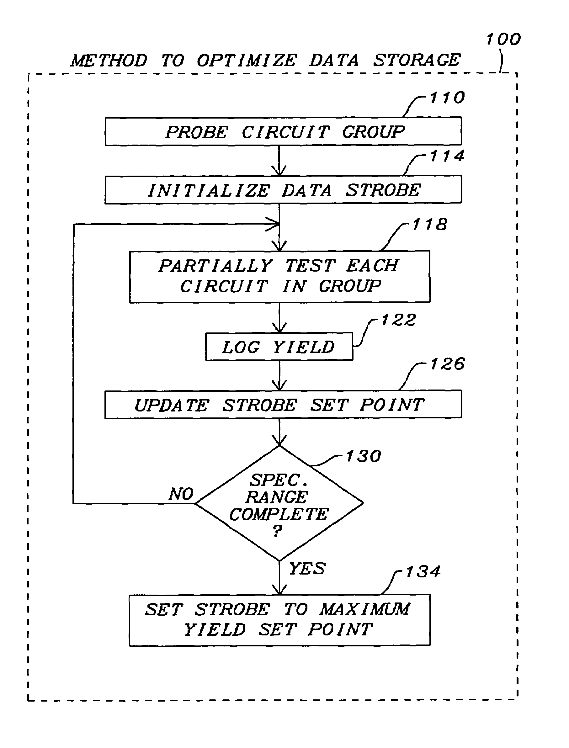
[0032]The preferred embodiments of the present invention disclose a method of testing a high speed data rate integrated circuit device. More particularly, a method of optimizing the data strobe for a parallel, multiple circuit, automated test system is disclosed. The method is applicable for either simultaneous, multiple die or multiple package testing. It should be clear to those experienced in the art that the present invention can be applied and extended without deviating from the scope of the present invention.

[0033]Referring now to FIG. 5, the first preferred embodiment of the present invention method 100 to optimize a data strobe for a multiple circuit, automatic test system is shown. Several important features of the present invention are shown in the illustration and are further describe below. The method 100 is particularly effective for improving circuit yield during a wafer test or during a packaged device final test. The method 100 comprises, first, probing, in parallel,...


PUM


Abstract

A method to optimize a data strobe for a multiple circuit, automatic test system is achieved. The method comprises, first, probing, in parallel, a circuit group wherein the circuit group comprises a plurality of circuits. Next, a data strobe of an automatic test system is initialized to a strobe set point relative to a system clock cycle. Next, the function of each of the circuits is partially tested, in parallel, using the strobe set point. Next, the circuit yield of the circuit group from the step of partially testing at the strobe set point is logged. Next, the data strobe is updated to a new strobe set point. Next, the steps of testing, logging, and updating are repeated until a specified range of strobe set points is completed. Finally, the data strobe is set for the circuit group to the strobe set point associated with the highest circuit yield.

Description

[0001]This is a division of patent application Ser. No. 10 / 167,858, filing date Jun. 11, 2002, now U.S. Pat. No. 6,943,044 assigned to the same assignee as the present inventionBACKGROUND OF THE INVENTION[0002](1) Field of the Invention[0003]The invention relates to a method to testing an integrated circuit device, and, more particularly, to a method of high speed data rate testing using an optimized data strobe for a parallel, multiple circuit, automated test system.[0004](2) Description of the Prior Art[0005]An important step in the manufacture of integrated circuit devices is testing. Due to the increasing complexity and speed of IC devices, testing presents unique challenges. Typically, IC devices are tested several times in the manufacturing sequence. In particular, individual IC die are tested at the wafer level, prior to sawing and packaging. The packaged parts are then re-tested to insure functionality.[0006]A challenging circuit testing scenario involves very high speed dev...

Claims


Application Information

Patent Timeline
Patent Type & Authority Patents(United States)
IPC IPC(8): G01R31/3177G01R31/40G11C5/00H01L21/66
CPCG01R31/31922G11C29/006G11C29/023G11C11/40G11C2029/5602
Inventor TING, TAH-KANG JOSEPHWANG, SHIH-HSINGCHEN, HONG-JIE
Owner ETRON TECH INC
Features
  • R&D
  • Intellectual Property
  • Life Sciences
  • Materials
  • Tech Scout
  • Unparalleled Data Quality
  • Higher Quality Content
  • 60% Fewer Hallucinations
Learn More