Semiconductor light-emitting device

a semiconductor and light-emitting technology, applied in the direction of semiconductor lasers, solid-state devices, lasers, etc., can solve the problems of poor adhesion with respect to pd/au, unstable kink level, easy to come off of zrosub>2 /sub>film, etc., to improve voltage resistance, improve adhesion, and reduce the effect of electric field concentration

Inactive Publication Date: 2009-01-13
ROHM CO LTD
View PDF12 Cites 6 Cited by
  • Summary
  • Abstract
  • Description
  • Claims
  • Application Information

AI Technical Summary

Benefits of technology

[0017]In order to overcome the problems described above, preferred embodiments of the present invention provide a semiconductor light-emitting device which minimizes the electric field concentration at the edge portion of the mesa portion on the p-type semiconductor layer by electric current from the p-type electrode layer so as improve voltage resistance, achieve good adhesion between the insulation film and the p-type electrode layer, and a stabilized kink level. Furthermore, preferred embodiments of the present invention provide a method for manufacturing a semiconductor light-emitting device which can increase the lift-off yield with respect to the p-type semiconductor layer.

Problems solved by technology

However, if a ZrO2 film is used as the insulation film 47, the ZrO2 film easily comes off because it has poor adhesion with respect to Pd / Au serving as the p-type electrode layer.
This makes the refraction index even higher in the vicinity of the middle of the mesa portion 53, which in turn causes generation of an undesirable transverse mode, resulting in an unstable kink level.
That is, it becomes difficult to generate single-transverse-mode oscillation by optimizing the design of the width of mesa portion 53 alone.
Furthermore, although there is a method to make the Al2O3 film sufficiently thinner than the light-emitting wavelength, if the Al2O3 film is too thin, it is unable to keep the film uniform, making it impossible to maintain adhesion to Pd / Au.

Method used


Image

  • Semiconductor light-emitting device
  • Semiconductor light-emitting device
  • Semiconductor light-emitting device

Examples


first preferred embodiment

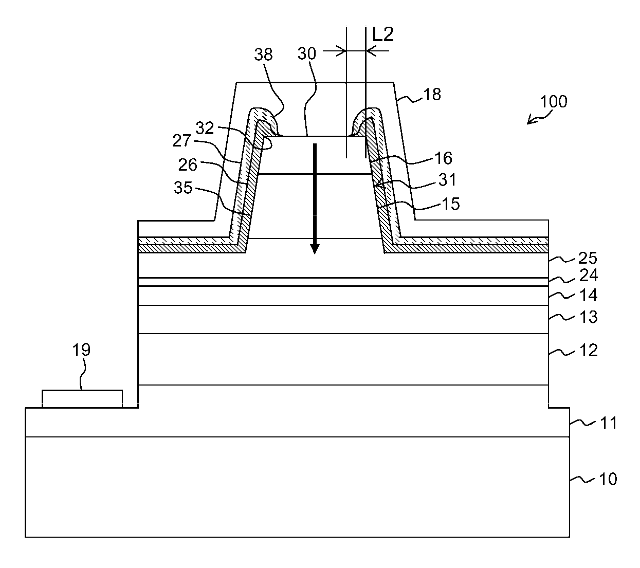
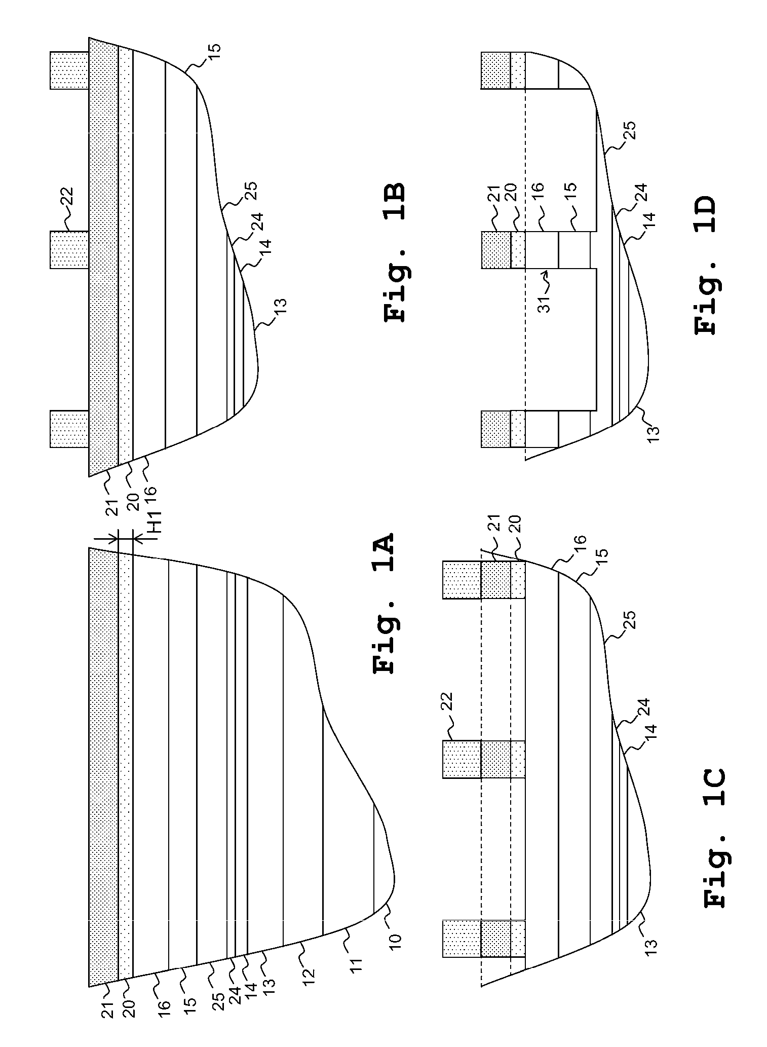
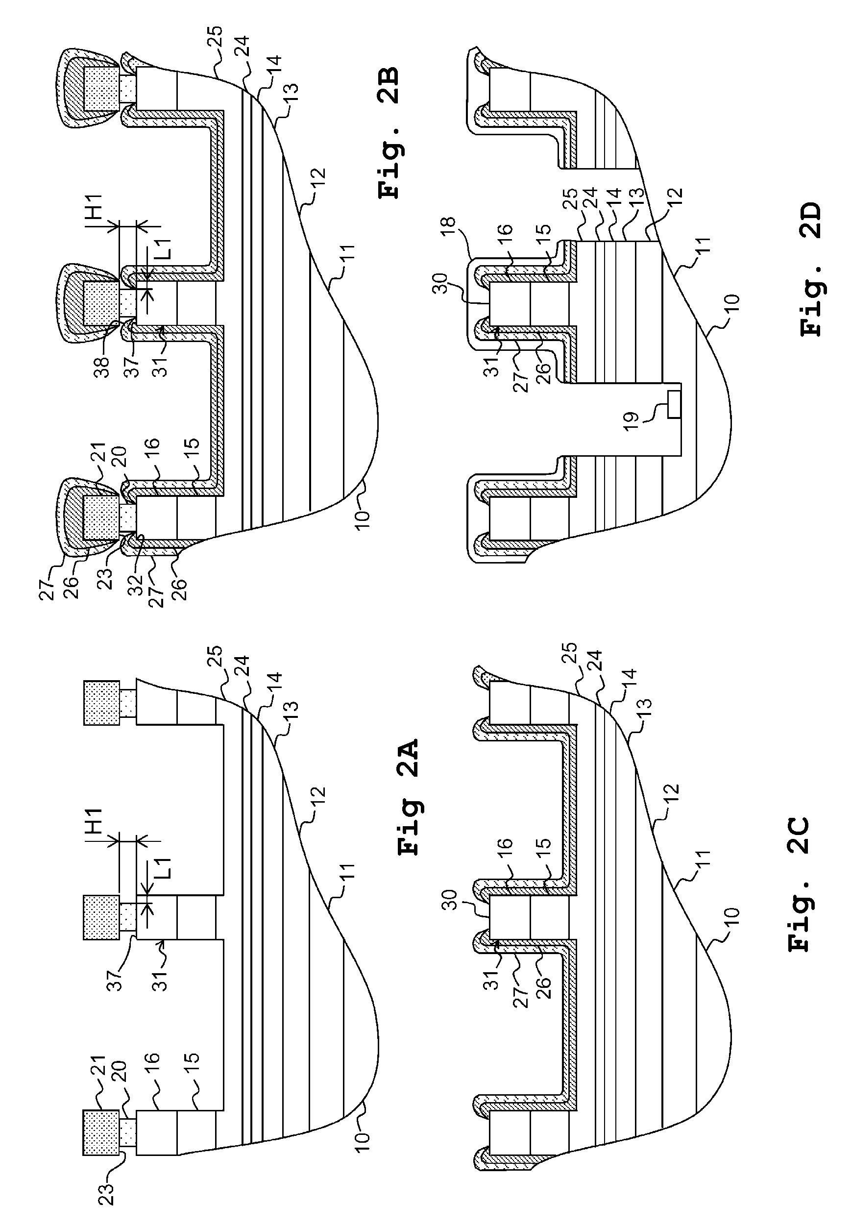
[0051]First, explanation will be made of the method for manufacturing a semiconductor light-emitting device according to the present preferred embodiment. FIGS. 1A to 1D and FIGS. 2A to 2D are schematic representations that show processes before forming the p-type electrode layer and the n-type electrode on a Group-III nitride-based compound semiconductor wafer expressed as AlxGayIn1-x-yN (where, 0≦x≦1; 0≦y≦1; 0≦x+y≦1). FIGS. 1A to 1D and FIGS. 2A to 2D indicate schematic cross-sectional views of a semiconductor light-emitting device in each process. It is noted that, in each figure, only a portion that requires the explanation of the method for manufacturing a semiconductor light-emitting device is described.

Mask Layer Forming Process

[0052]In the manufacturing method of a semiconductor light-emitting device according to the present preferred embodiment, a semiconductor light-emitting device of a Group-III nitride-based compound semiconductor expressed as AlxGayIn1-x-yN (where, 0≦x≦...

second preferred embodiment

[0082]Next, discussion will be made of another preferred embodiment of the method of manufacturing a semiconductor light-emitting device. FIG. 8A through FIG. 11D are schematic representations showing processes to form a p-type electrode layer and an n-type electrode layer on a wafer of a Group-III nitride-based compound semiconductor expressed as AlxGayIn1-x-yN (where, 0≦x≦1; 0≦y≦1; 0≦x+y≦1), and to complete a semiconductor light-emitting device. In addition, FIGS. 12A and 12B are schematic representations of a manufacturing process of a semiconductor light-emitting device according to another preferred embodiment. FIG. 8A through FIG. 11D show schematic sectional views of the semiconductor light-emitting device in each process. In addition, in FIGS. 12A through 12B show schematic sectional views of the semiconductor light-emitting device in each process. It is noted that in FIG. 8A through FIG. 12B, only a single-unit semiconductor light-emitting device is described, but this can ...


PUM


Abstract

A semiconductor light-emitting device and method for manufacturing the semiconductor light-emitting device includes a mask layer etching process on first and second mask layers provided on a Group-III nitride-based compound semiconductor substrate, the mask layer with a higher etching rate being closer to the p-type semiconductor layer; a semiconductor layer etching process; a side-etching process that selectively etches the side of the mask layer with the high etching rate to define a groove portion with a portion of the p-type semiconductor layer exposed; a ZrO2 film forming process that forms a ZrO2 film so as to cover the exposed p-type semiconductor layer; an Al2O3 film forming process that forms an Al2O3 film so as to cover the ZrO2 film; a mask layer removing process; and an electrode layer forming process. The method for manufacturing the semiconductor light-emitting device increases the yield of lift-off with respect to the p-type semiconductor layer and can produce a semiconductor light-emitting device with an improved voltage resistance.

Description

BACKGROUND OF THE INVENTION[0001]1. Field of the Invention[0002]The present invention relates to a method for manufacturing a semiconductor light-emitting device equipped with a semiconductor light-emitting element and to a semiconductor light-emitting device.[0003]2. Description of the Related Art[0004]Conventionally, a semiconductor light-emitting device composed of a Group-III nitride-based compound semiconductor expressed by AlxGayIn1-x-yN (where, 0≦x≦1; 0≦y≦1; 0≦x+y≦1) has been manufactured as follows.[0005]FIG. 7 shows a schematic block diagram of a semiconductor light-emitting device obtained by a conventional manufacturing method.[0006]In a conventional process of manufacturing a semiconductor light-emitting device, an SiO2 film is formed on the top surface of p-GaN contact layer 46 of a semiconductor substrate having n-GaN contact layer 41, n-AlGaN clad layer 42, n-GaN guide layer 43, InGaN / GaN active layer 44, p-AlGaN electronic block layer 55, p-GaN guide layer 56, p-AlGa...

Claims


Application Information

Patent Timeline
Patent Type & Authority Patents(United States)
IPC IPC(8): H01L29/26H01S5/042H01S5/22H01S5/343
CPCB82Y20/00H01S5/34333H01L33/20H01L33/38H01S5/0425H01S5/2009H01S5/22H01S2304/12H01S5/04257H01S5/04254H01S2301/176
Inventor MURAYAMA, MASAHIRO
Owner ROHM CO LTD
Why Eureka
Try Eureka