Photoresist system

a photoresist system and photolithography technology, applied in the field of semiconductor foundry, can solve the problem of lithography process not being allowed to continue, and achieve the effect of saving semiconductor foundry money and customer goodwill

Inactive Publication Date: 2009-01-13
TAIWAN SEMICON MFG CO LTD
View PDF10 Cites 1 Cited by
  • Summary
  • Abstract
  • Description
  • Claims
  • Application Information

AI Technical Summary

Problems solved by technology

Beneficially, improperly performed operations relating to switching photoresist bottles are detected, so that semiconductor wafers are not damaged, saving the semiconductor foundry money and customer goodwill.
That is, if the wrong type of photoresist is inserted, or if an expired bottle of photoresist is inserted, the condition is detected, and the lithography process not allowed to continue until the condition is rectified.

Method used


Image

  • Photoresist system
  • Photoresist system
  • Photoresist system

Examples


Embodiment Construction

[0014]In the following detailed description of exemplary embodiments of the invention, reference is made to the accompanying drawings that form a part hereof, and in which is shown by way of illustration specific exemplary embodiments in which the invention may be practiced. These embodiments are described in sufficient detail to enable those skilled in the art to practice the invention. Other embodiments may be utilized, and logical, mechanical, and other changes may be made without departing from the spirit or scope of the present invention. The following detailed description is, therefore, not to be taken in a limiting sense, and the scope of the present invention is defined only by the appended claims.

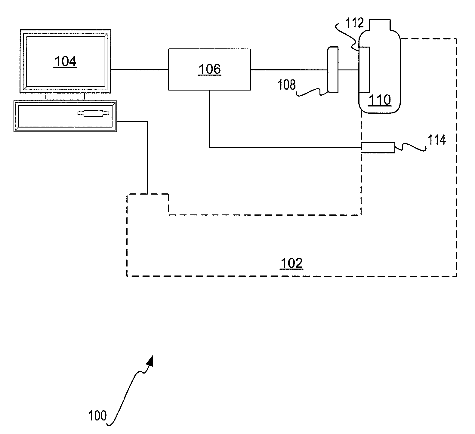
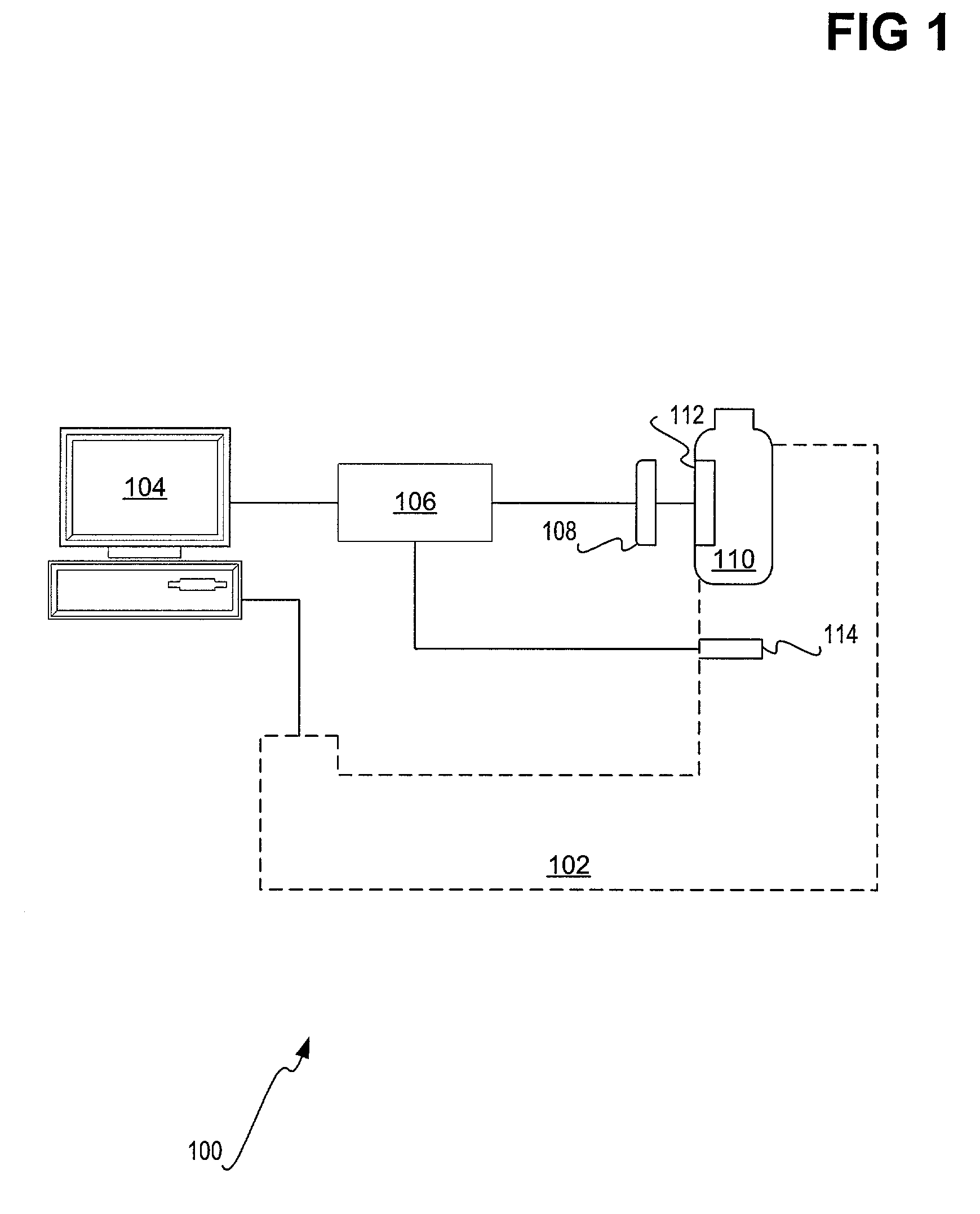
[0015]FIG. 1 shows the hardware system architecture of an embodiment of the invention. The hardware system 100 includes a photo track 102, a fabrication computer 104, a controller 106, a barcode reader 108, and a bottle sensor 114. The photo track 102 is the lithography photoresist...


PUM

PropertyMeasurementUnit
length of timeaaaaaaaaaa
polarityaaaaaaaaaa

Abstract

A photoresist system is disclosed. A graphical user interface of the system allows an operator to initiate a bottle switching operation, among other operations. Barcode data of a photoresist bottle is obtained by an equipment server from a controller. Photoresist data relating to the bottle is obtained by the equipment server from a database through a constraint server. The equipment server, preferably with assistance from the constraint server, determines whether the bottle contains appropriate photoresist for the semiconductor processing to be performed on semiconductor wafers. If the bottle contains appropriate photoresist, the equipment server, through the constraint server, stores the expiration date of the bottle and the batch identifier of the bottle, as indicated by the barcode data, in the database. If the bottle contains inappropriate photoresist, then the system acts to prevent the semiconductor processing of the semiconductor wafers with the inappropriate photoresist contained in the bottle.

Description

FIELD OF THE INVENTION[0001]This invention relates generally to semiconductor fabrication, and more particularly to the photolithography that may be performed during such fabrication.BACKGROUND OF THE INVENTION[0002]Photoresist is the light-sensitive film typically spun onto semiconductor wafers and exposed using high-intensity light through a photomask. The exposed photoresist (or the unexposed photoresist, depending on the polarity of the resist) is dissolved with developers, leaving a pattern of photoresist that allows etching to take place in some areas of the wafer, while preventing it in other areas of the wafer. Thus, photoresist is used in semiconductor fabrication primarily in the lithography or photolithography stages. Lithography itself generally is the process of pattern transfer.[0003]Photoresist comes in different types, for different applications. For example, photoresist may be positive or negative photoresist, which generally indicates its amenability to being devel...

Claims


Application Information

Patent Timeline
Patent Type & Authority Patents(United States)
IPC IPC(8): G06F19/00G03F7/16G03F7/20
CPCG03F7/70541G03F7/16
Inventor YANG, YENNIYEH, FU-KAI
Owner TAIWAN SEMICON MFG CO LTD
Why Eureka
Try Eureka