Read write device for optical memory and method therefore

a write device and optical memory technology, applied in the direction of instruments, pharmaceutical product form changes, disposition/mounting of heads, etc., can solve the problems of source weight, large size, and certain limitations of the opu system of prior art, and achieve the effect of reliable operation, small size and low weight of the optical storage system

Inactive Publication Date: 2009-01-20
NOKIA CORP
View PDF26 Cites 82 Cited by
  • Summary
  • Abstract
  • Description
  • Claims
  • Application Information

AI Technical Summary

Benefits of technology

[0008]An object of the present invention is to solve the problems related to prior art and thus to provide a device and method for reading out data from the optical storage medium and writing data to the optical storage medium enabling a small-size and low-weight optical storage system. Another object of the invention is to provide a method and device for reading out data from the optical storage medium and writing data to the optical storage medium to keep an optical storage system in focus and on track to ensure a reliable operation.
[0014]The present invention provides a novel way of implementing the optical read / write system which enables to reduce component count by a new optical component arrangement which simplifies the optical system. The moving access unit according to the present invention is possible to manufacture using thinner geometries and thus the moving acces unit fulfils the requirements of small size and low weight which are crucial needs in the ultraminiature range of optical storage devices.
[0015]In addition, the present invention provides a novel and accurate way of keeping the optical read / write system in focus and on track. The combination of using transversal light beams to be directed to and reflected from the optical storage medium and the use of the moving access unit provides a simple focusing and tracking method. The focus-error and track-error signals can be identified by following the change in the intensity distribution of the reflected light beam. The reliable operation is achieved by the simultaneous transversal light beam focusing and tracking during the read and / or write operation.
[0016]In addition, a smaller size and lower weight of the moving access unit according to the present invention also enables faster random access time of the optical storage device. The movable mass of the access unit becomes still lighter by fixing all possible components (including a light source) onto the pivot point of the access unit. This minimizes the angular momentum needed to move the arm. By reducing component count the method and device according to the invention thus reduces power consumption. The component count of optical components can be minimized in the simplest implementation of the present invention significantly. Due to reduced component count space savings are also achieved and production costs become lower.

Problems solved by technology

There are certain limitations related to the OPU systems of prior art.
A mass of the movable OPU or the geared rotatably positioned optical light guide head is heavy.
Especially a laser source is a weighty and large-size component and the mass of the laser source is centered on the movable OPU or the movable light guide head in prior art systems.
The weight of the movable OPU causes together with the pitching motion of the disc problems in defocussing and sensitivity to the track angle error.
Many optical storage systems of prior art require astigmatism in the system for error analysis, and this also results in higher component count in the form of used astigmatism elements.
All extra components cause weight increase and complexity to the system which extends access times and increases power consumption of the OPU system.

Method used


Image

  • Read write device for optical memory and method therefore
  • Read write device for optical memory and method therefore
  • Read write device for optical memory and method therefore

Examples


Embodiment Construction

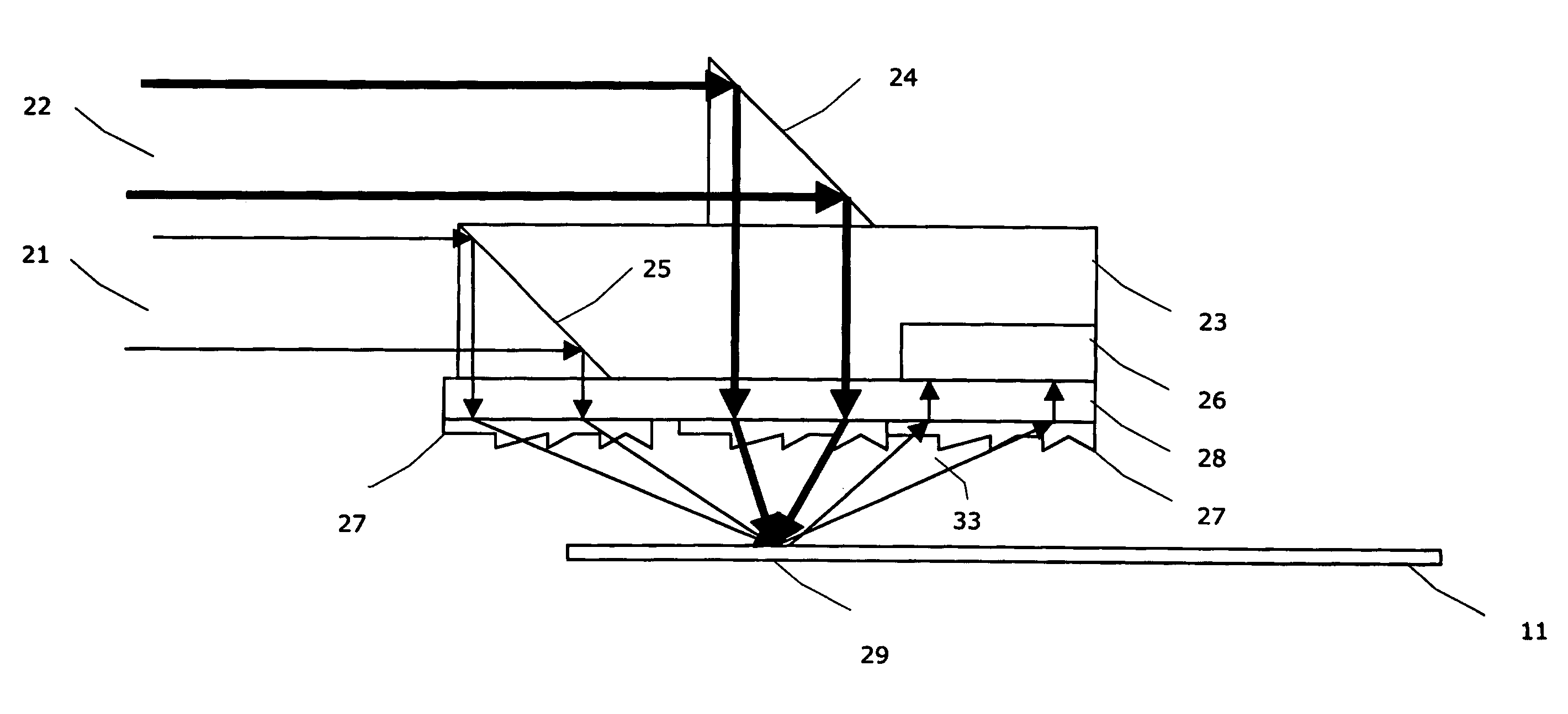
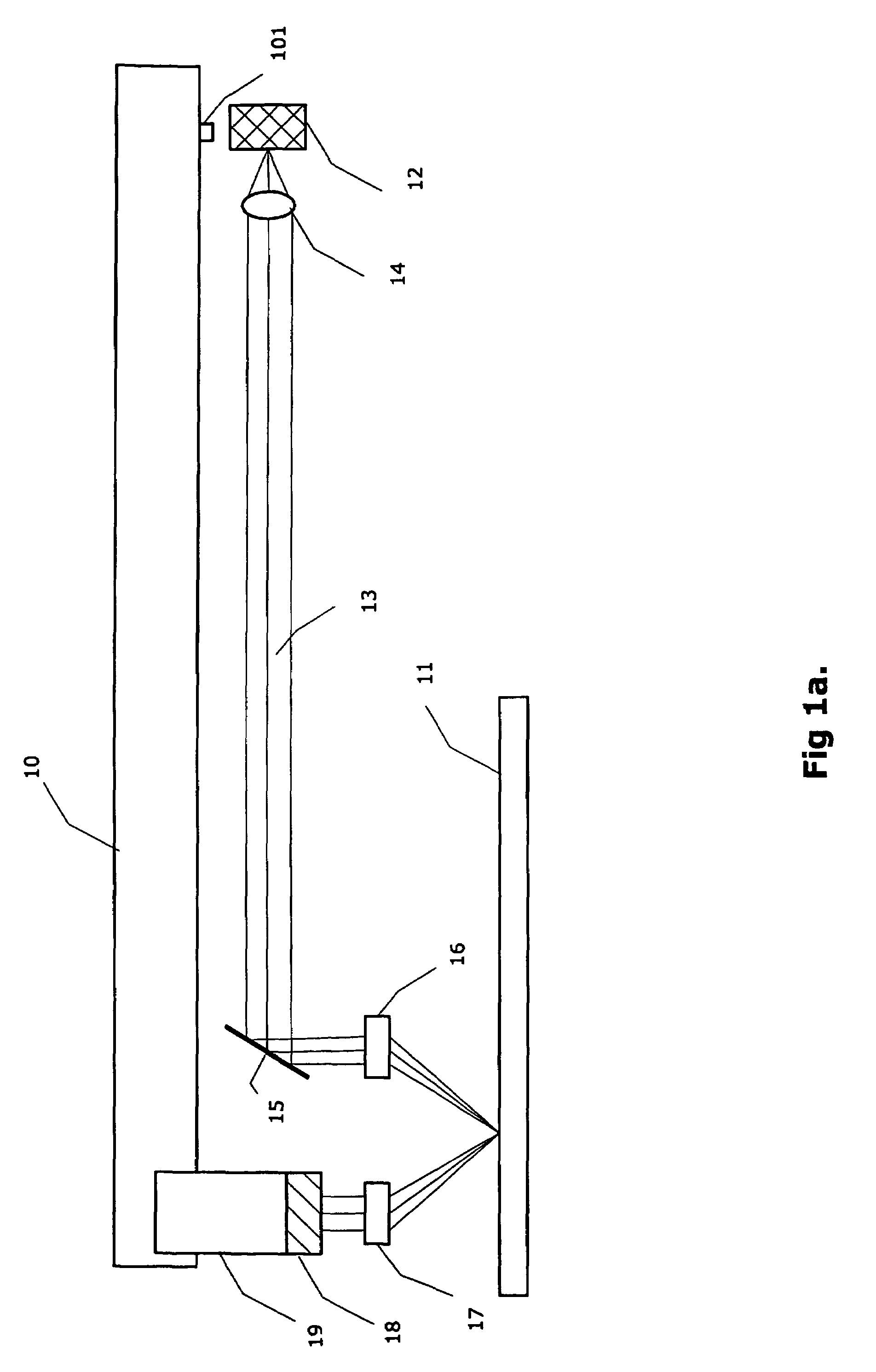
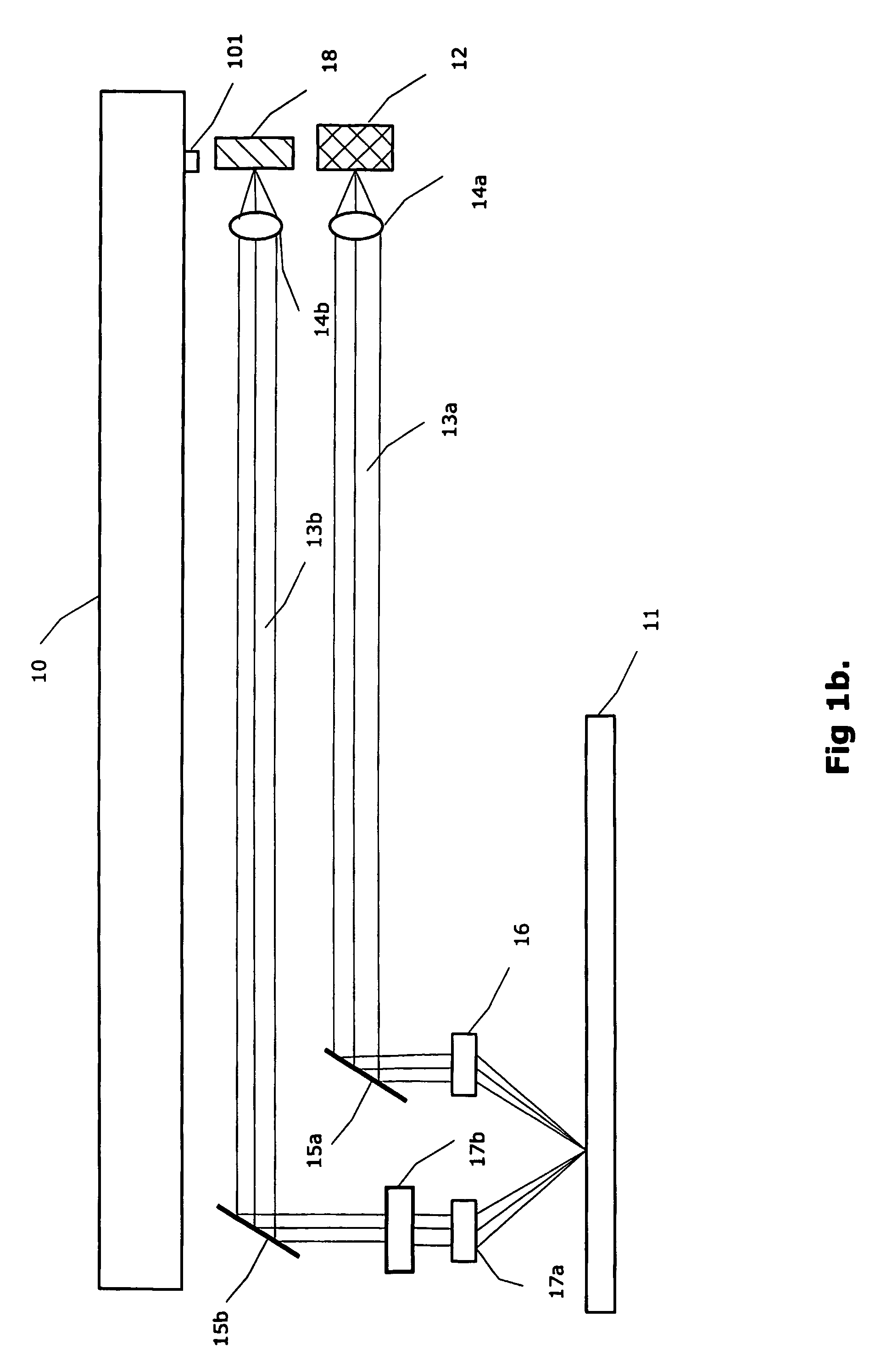
[0051]FIG. 1a illustrates a principal set up of the device according to the present invention for reading out data from an optical storage medium and for writing data to an optical storage medium. The optical storage medium 11 can be any CD-type readable and / or writeable optical disc, such as CD-R, CD-ROM, CD-RW, DVD or any other existing optical disc media or future implementations of this kind. The optical storage medium 11 comprises data tracks, and adjacent data tracks are decoupled from each other by a narrow area. The data tracks may be pre-grooved or stamped and made of suitable material to form optically resolvable structures on the optical storage medium. Bit patterns that produce adequate optical intensity variation on the data tracks, e.g. the pitted structure of the medium, form a basis for storing and changing information. The device also comprises an optical storage medium drive (not depicted), which can be of any commercial type available. The movement of the optical ...


PUM

PropertyMeasurementUnit
wavelengthsaaaaaaaaaa
time periodaaaaaaaaaa
massaaaaaaaaaa

Abstract

A method and miniaturizable device is described to read / write information to an optical storage medium (11). A device comprises one or more light sources (12) bounded up with an access unit (10) which is arranged to be controllable to a position, in which light beams (21, 22) are transmitted transversal towards an optical storage medium, and reflected light beams (33) are analysed by a detector element (18, 26) which further informs the access unit whether to move or stand still to keep light beams in focus and on track. A device according to the invention is possible to implement in a small size and low weight due to reduced component count and thin access unit geometries. A communication device (80) according to the invention may be implemented to fulfil a crucial need for ultraminiature range of communication devices.

Description

CROSS REFERENCE TO RELATED APPLICATIONS[0001]This application is for entry into the U.S. national phase under §371 for International Application No. PCT / FI02 / 000954 having an international filing date of Nov. 27, 2002, and from which priority is claimed under all applicable sections of Title 35 of the United States Code including, but not limited to, Sections 120, 363 and 365(c).TECHNICAL FIELD OF THE INVENTION[0002]The present invention relates to the field of optical storage systems, and more particularly to reading out information from an optical storage medium and to writing information onto the optical storage medium.BACKGROUND OF THE INVENTION[0003]An optical storage system is composed of an optical disc drive system and an optical storage medium, such as an optical disc. The optical disc drive has a light beam source, a light beam distribution system and a light beam detection system for reading out information from the optical disc and recording information onto the optical ...

Claims


Application Information

Patent Timeline
Patent Type & Authority Patents(United States)
IPC IPC(8): G11B7/00A61J3/06A61K9/20B29C43/08B29C43/36B30B11/08G11B7/08G11B7/085G11B7/09G11B7/135G11B7/14
CPCG11B7/08576G11B7/135G11B7/14G11B7/0901G11B7/0912
Inventor MAKELA, JAKKEAIKIO, JANNE KARIAIKIO, SANNAKATAJA, KARI JUHANIALAJOKI, TEEMU
Owner NOKIA CORP
Why Eureka
Try Eureka