TFT array panel having a two-portion coupling electrode extending from drain electrode in different directions with first portion extending along a gap between two overlapping subpixel electrodes thereon and second portion extending in same direction as data line

a technology of drain electrode and array panel, which is applied in the field of liquid crystal display, can solve the problems of lcd image quality being affected by viewing direction, lcd image may have poor quality when viewed from the side as compared to when viewed from the front, and the luminance difference between high grays disappearing, so as to reduce gray scale inversion and improve lateral visibility

Inactive Publication Date: 2009-02-03
SAMSUNG DISPLAY CO LTD
View PDF8 Cites 1 Cited by
  • Summary
  • Abstract
  • Description
  • Claims
  • Application Information

AI Technical Summary

Benefits of technology

[0008]The present invention provides an LCD that may reduce gray scale inversion at wider viewing angles, thereby improving lateral visibility.

Problems solved by technology

However, the LCD has a viewing direction dependency due to the refractive anisotropy.
In particular, the LCD image may have poor quality when viewed from the side as compared to when viewed from the front.
In the worse case, the luminance difference between high grays vanishes such that the images cannot be perceived.

Method used


Image

  • TFT array panel having a two-portion coupling electrode extending from drain electrode in different directions with first portion extending along a gap between two overlapping subpixel electrodes thereon and second portion extending in same direction as data line
  • TFT array panel having a two-portion coupling electrode extending from drain electrode in different directions with first portion extending along a gap between two overlapping subpixel electrodes thereon and second portion extending in same direction as data line
  • TFT array panel having a two-portion coupling electrode extending from drain electrode in different directions with first portion extending along a gap between two overlapping subpixel electrodes thereon and second portion extending in same direction as data line

Examples


Embodiment Construction

[0024]The present invention now will be described more fully hereinafter with reference to the accompanying drawings, which show exemplary embodiments of the invention. The present invention may, however, be embodied in many different forms and should not be construed as limited to the embodiments set forth herein.

[0025]In the drawings, the thickness of layers, films and regions are exaggerated for clarity. Like numerals refer to like elements throughout. It will be understood that when an element such as, for example, a layer, film, region or substrate is referred to as being “on” another element, it can be directly on the other element or intervening elements may also be present. In contrast, when an element is referred to as being “directly on” another element, there are no intervening elements present.

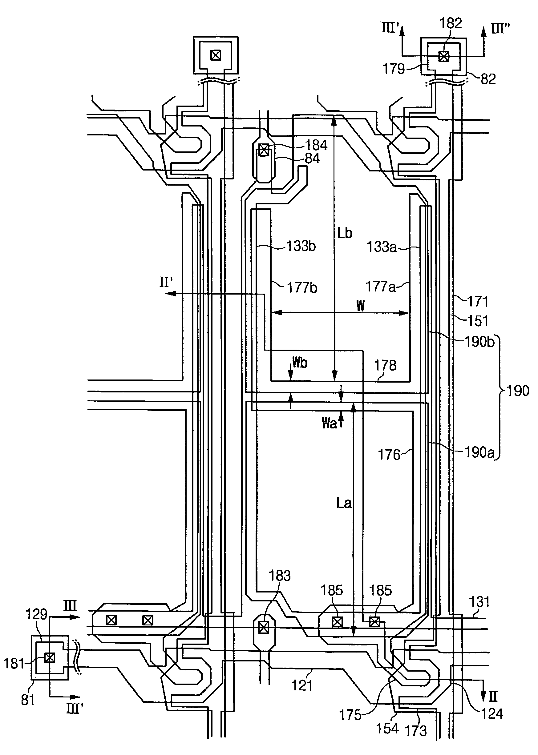
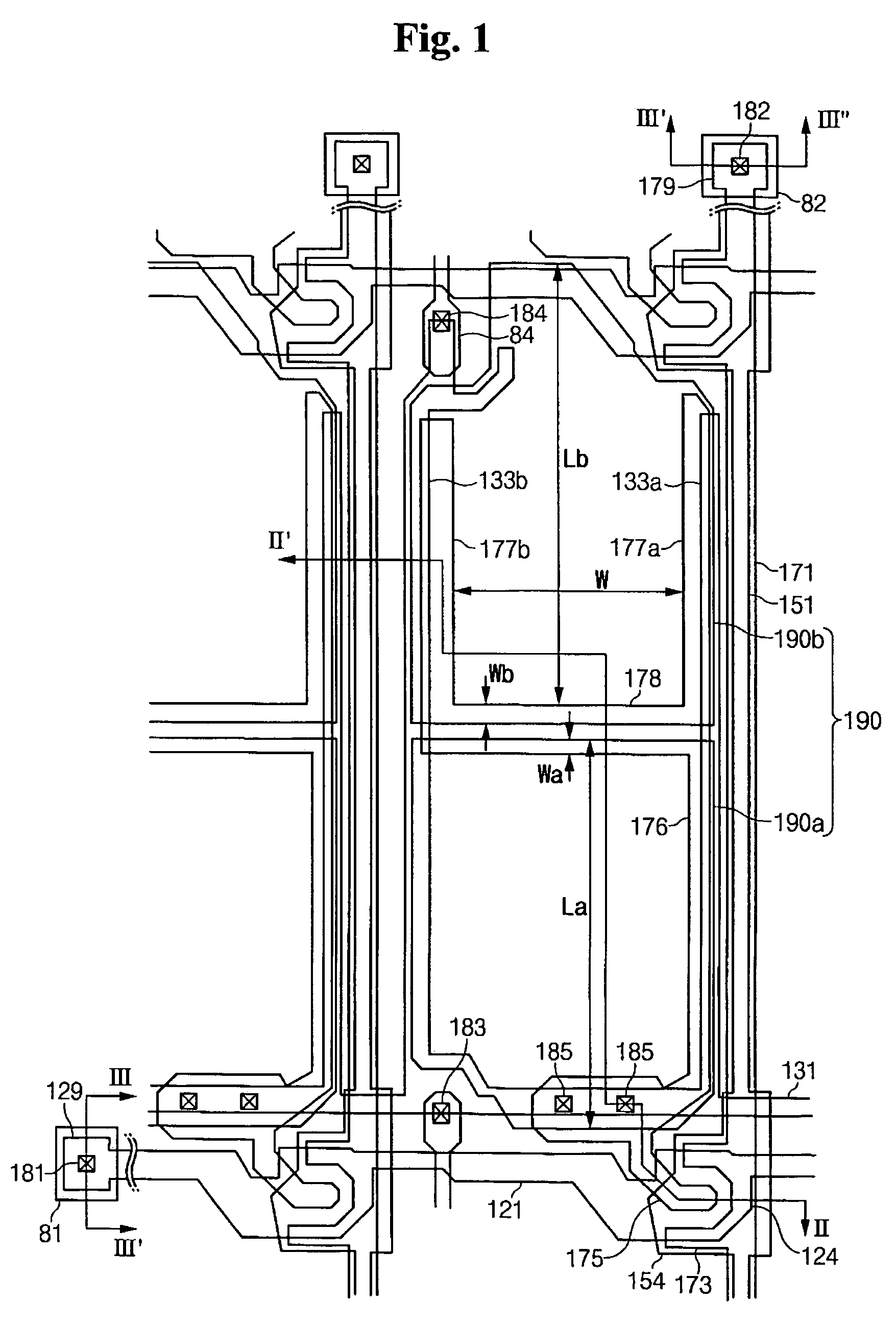
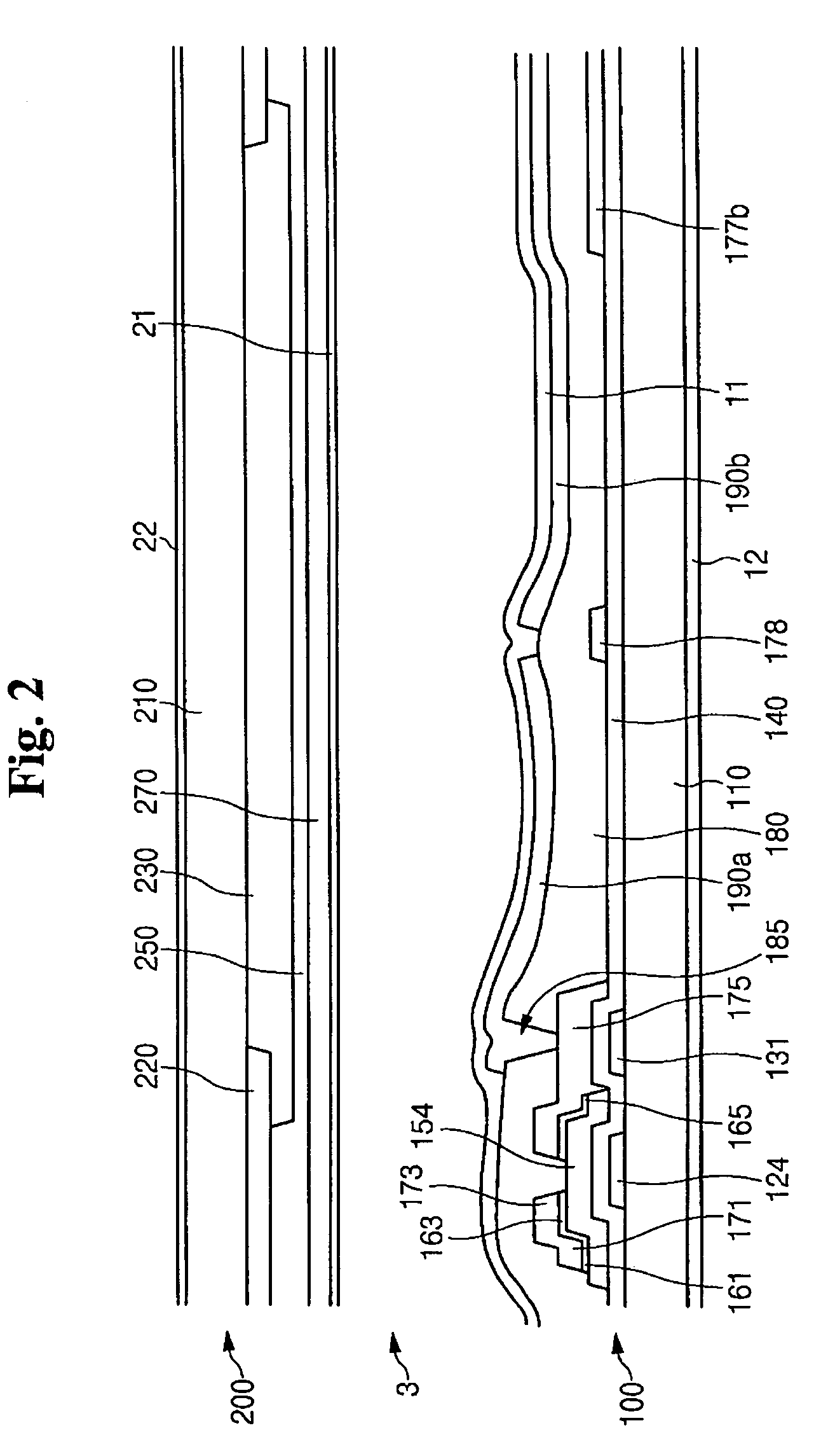
[0026]An LCD according to an exemplary embodiment of the present invention is described in detail with reference to FIG. 1, FIG. 2, and FIG. 3.

[0027]FIG. 1 is a layout view showing...


PUM

PropertyMeasurementUnit
angleaaaaaaaaaa
anglesaaaaaaaaaa
dielectric constantaaaaaaaaaa

Abstract

A thin film transistor array panel including a substrate; a gate line formed on the substrate; a gate insulating layer formed on the gate line; a semiconductor layer formed on the gate insulating layer; a data line formed on the semiconductor layer; a drain electrode separated from the data line and formed on the semiconductor layer; a coupling electrode connected to the drain electrode; a first subpixel electrode connected to the drain electrode; and a second subpixel electrode separated from the first subpixel electrode and overlapping the coupling electrode.

Description

CROSS REFERENCE TO RELATED APPLICATION[0001]This application claims priority to and the benefit of Korean Patent Application No. 10-2004-0024071, filed on Apr. 8, 2004, which is hereby incorporated by reference for all purposes as if fully set forth herein.BACKGROUND OF THE INVENTION[0002]1. Field of the Invention[0003]The present invention relates to a liquid crystal display. More particularly, this invention relates to an arrangement of pixel electrodes and capacitors in a pixel of a liquid crystal display.[0004]2. Discussion of the Background[0005]A liquid crystal display (LCD) is one of the most widely used flat panel displays. Generally, an LCD includes two panels having field-generating electrodes, such as pixel is electrodes and a common electrode, and a liquid crystal (LC) layer interposed between the two panels. The LCD displays images by applying voltages to the field-generating electrodes to generate an electric field in the LC layer, which determines LC molecule orientat...

Claims


Application Information

Patent Timeline
Patent Type & Authority Patents(United States)
IPC IPC(8): G02F1/136G02F1/1343G02F1/1362G02F1/1368G09F9/30H01L21/336H01L29/786
CPCG02F1/136213G02F2001/134345G02F1/134345B24B15/04B24B27/0023B24B37/11
Inventor HONG, SUNG-KYUKIM, JOO-HANLYU, JAE-JINHONG, SUNG-HWANLEE, WON-JAE
Owner SAMSUNG DISPLAY CO LTD
Why Eureka
Try Eureka