Semiconductor laser micro-heating element structure

a technology of micro-heating elements and semiconductor lasers, applied in semiconductor lasers, instruments, optics, etc., can solve problems such as difficulty in packaging fabrication, and achieve the effect of optimum output power and without excessive nois

Inactive Publication Date: 2009-02-03
CORNING INC
View PDF12 Cites 19 Cited by
  • Summary
  • Abstract
  • Description
  • Claims
  • Application Information

AI Technical Summary

Problems solved by technology

Accordingly, it is difficult to fabricate a package where the laser diode and the SHG crystal are perfectly wavelength matched.

Method used


Image

  • Semiconductor laser micro-heating element structure
  • Semiconductor laser micro-heating element structure
  • Semiconductor laser micro-heating element structure

Examples


Embodiment Construction

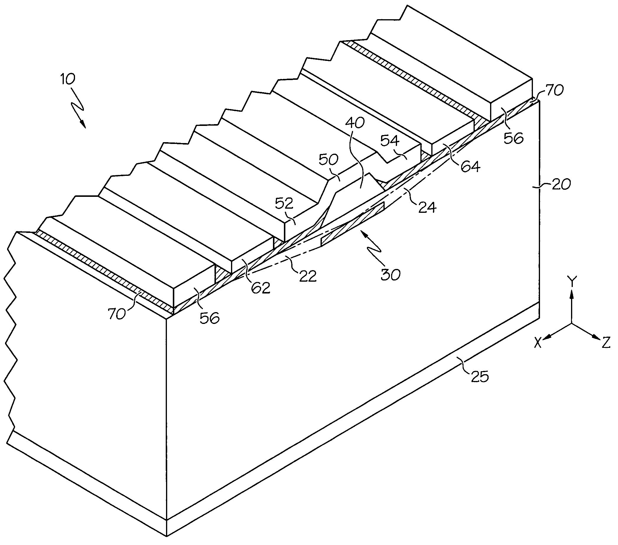
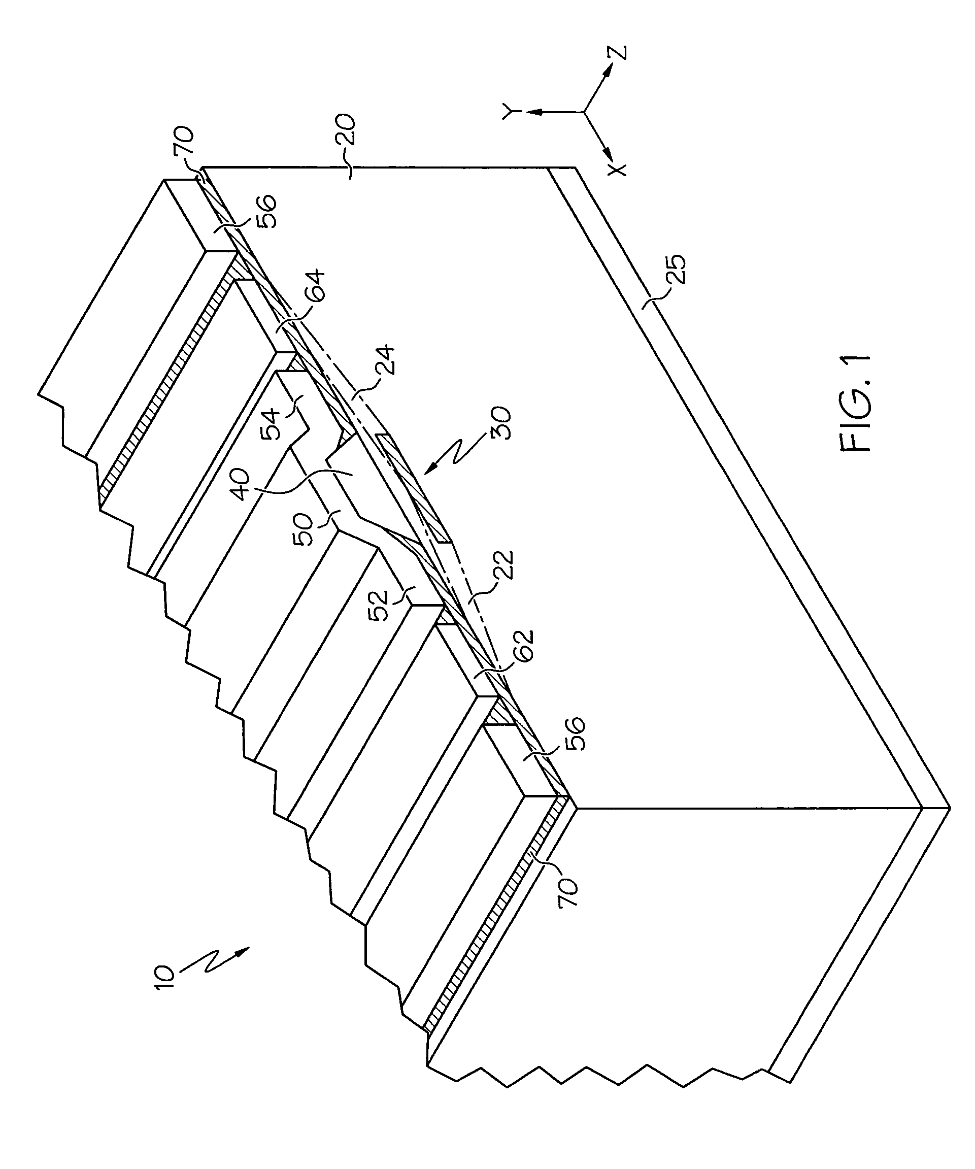
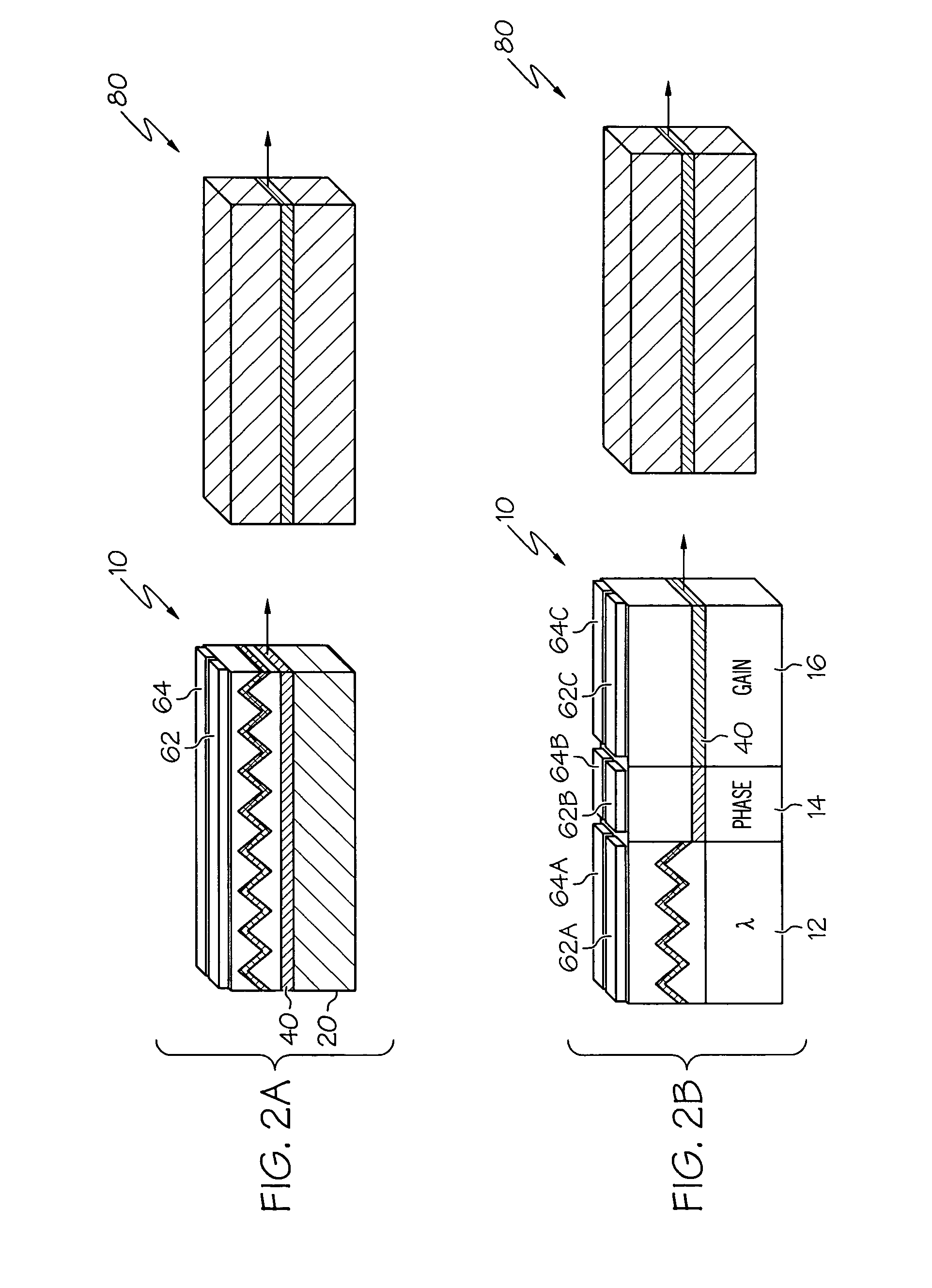
[0018]Referring to FIG. 1, it is noted that a semiconductor laser 10 according to the present invention may preferably comprise a semiconductor substrate 20 including an active region 30, a ridge waveguide 40, a driving electrode structure, and a micro-heating element structure. In the illustrated embodiment, the driving electrode structure comprises a driving electrode element 50 and the micro-heating element structure comprises a pair of heating element strips 62, 64. The active region 30 is defined by P and N type semiconductor material within the semiconductor substrate 20 and is configured for stimulated emission of photons under an electrical bias VBIAS generated by the driving electrode element 50 and a corresponding N-Type region 25 defined in the substrate 20. The wavelength output of the semiconductor laser 10 is dependent upon the temperature of the ridge waveguide 40 and the active region 30 and the micro-heating element structure is configured to alter the temperature o...


PUM


Abstract

A semiconductor laser is provided comprising a semiconductor substrate, an active region, a ridge waveguide, a driving electrode structure, and a micro-heating element structure. The micro-heating element structure comprises a pair of heating element strips extending along the longitudinal dimension of the semiconductor laser. The heating element strips are on opposite sides of the ridge waveguide such that one of the heating element strips extends along one side of the ridge waveguide while a remaining heating element strip extends along another side of the ridge waveguide.

Description

CROSS-REFERENCE TO RELATED APPLICATIONS[0001]This application claims the benefit of priority under 35 U.S.C. § 119(e) of U.S. Provisional Application Ser. No. 60 / 833,531 filed on Jul. 26, 2006, the content of which is relied upon and incorporated herein by reference in its entirety.BACKGROUND OF THE INVENTION[0002]The present invention relates generally to semiconductor lasers and, more particularly to the control of temperature in specific regions of a semiconductor laser.SUMMARY OF THE INVENTION[0003]The present invention relates generally to semiconductor lasers, which may be configured in a variety of ways. For example, and by way of illustration, not limitation, short wavelength sources can be configured for high-speed modulation by combining a single-wavelength semiconductor laser, such as a distributed-feedback (DFB) laser or a distributed-Bragg-reflector (DBR) laser, with a light wavelength conversion device, such as a second-harmonic-generation (SHG) crystal. The SHG crysta...

Claims


Application Information

Patent Timeline
Patent Type & Authority Patents(United States)
IPC IPC(8): H01S3/04H01S5/12
CPCH01S5/0261H01S5/0612H01S5/06256G02F1/37H01S5/0425H01S5/12H01S5/22H01S5/2231H01S5/04256
Inventor HU, MARTIN HAILIU, XINGSHENGZAH, CHUNG-EN
Owner CORNING INC
Why Eureka
Try Eureka