Thin-film lithium niobate-based integrated chip and preparation method thereof

An integrated chip and lithium niobate technology, applied in nonlinear optics, instruments, optics, etc., can solve the problems of poor passband shape of the filter, difficulty in application, low stability and reliability, etc., to achieve accurate splitting ratio, The effect of large working bandwidth

Inactive Publication Date: 2020-10-02
南京中电芯谷高频器件产业技术研究院有限公司
View PDF2 Cites 17 Cited by
  • Summary
  • Abstract
  • Description
  • Claims
  • Application Information

AI Technical Summary

Problems solved by technology

[0003] Traditional microwave photonic signal processing is built with discrete devices, which has low stability and reliability and is difficult to implement
With the development of silicon-based photonics, silicon-based photonic chips based on CMOS technology can achieve monolithic integration of electro-optic modulators, microring filters, photodetectors, etc. (Weifeng Zhang and Jianping Yao, On-chipsilicon photonic integrated frequency-tunable bandpass microwave photonicfilter, Opt.Lett.43, 3622-3625), realizes the filter function, adopts the principle based on phase modulation to intensity modulation to realize the bandpass filter, but the shape of the passband of the filter is poor, unable to Realize the ideal rectangular bandpass filtering effect, and the bandwidth performance of the silicon-based modulator is lower than that of the traditional bulk lithium niobate modulator

Method used


Image

  • Thin-film lithium niobate-based integrated chip and preparation method thereof
  • Thin-film lithium niobate-based integrated chip and preparation method thereof
  • Thin-film lithium niobate-based integrated chip and preparation method thereof

Examples


preparation example Construction

[0050] Its preparation method specifically comprises the following steps:

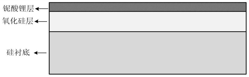
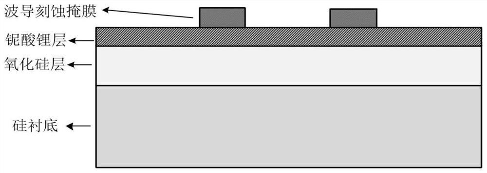
[0051] 1) On the silicon-based thin film lithium niobate substrate material, the waveguide pattern mask is prepared by electron beam exposure technology. The electron beam glue adopts HSQ negative glue with a thickness of 500-800 nanometers, such as figure 1 , figure 2 shown;

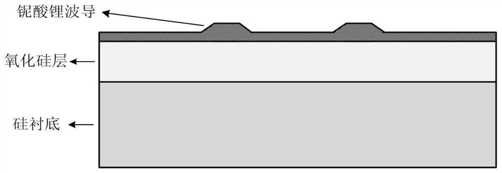
[0052] 2) The lithium niobate waveguide is prepared by inductively coupled plasma etching based on sulfur hexafluoride gas, and the etching depth is 250-350 nm, such as image 3 shown;

[0053] 3) Using plasma-enhanced chemical vapor deposition to grow a silicon oxide upper cladding layer with a thickness of 1-3 microns, such as Figure 4 shown;

[0054] 4) The photoresist pattern of the dielectric hole is prepared by planar photolithography and development technology. The photoresist can be selected from AZ 7908, AZMIR 701 or AZ 4562, the thickness is greater than the thickness of the silicon oxide cladding, and the photor...

Embodiment 1

[0058] The filtering and delay implementation methods are as follows:

[0059] 1) Initial state debugging: first adjust U1 to adjust the first ring to an over-coupling state, then adjust U3 and U4 to adjust the resonance wavelengths of the two resonant cavities to be the same, that is, adjust to a resonance peak, and adjust U2 to adjust the second The ring is tuned to an over-coupling state.

[0060] 2) Bandwidth-tunable filtering: In the initial state, change U2 (in the over-coupling state), and fine-tune U1 accordingly to achieve a filter response with a constant central wavelength and adjustable bandwidth, such as Figure 9 shown.

[0061] 3) Adjustable central wavelength filtering: In the initial state, change U1 to achieve a filter response with constant bandwidth and adjustable central wavelength, such as Figure 10 shown.

[0062] 4) Simultaneously adjustable bandwidth and center wavelength filtering: In the initial state, change U2 (in the over-coupling state) and U...

Embodiment 2

[0068] A method for preparing a thin-film lithium niobate-based integrated chip, specifically comprising the following steps:

[0069] 1) On the silicon-based thin-film lithium niobate substrate material, the mask of the waveguide pattern is prepared by electron beam exposure technology. The electron beam glue uses HSQ negative glue with a thickness of 600 nanometers, such as figure 1 , figure 2 shown;

[0070] 2) The lithium niobate waveguide was prepared by inductively coupled plasma etching based on sulfur hexafluoride gas, with an etching depth of 300 nm, such as image 3 shown;

[0071] 3) Using plasma-enhanced chemical vapor deposition to grow a silicon oxide upper cladding layer with a thickness of 2 microns, such as Figure 4 shown;

[0072] 4) The photoresist pattern of the dielectric hole is prepared by planar photolithography and development technology. The photoresist is AZ MIR 701 with a thickness of 2.5 microns, and the electrodes are etched by inductively c...


PUM

PropertyMeasurementUnit
thicknessaaaaaaaaaa
thicknessaaaaaaaaaa
thicknessaaaaaaaaaa

Abstract

The invention discloses a thin-film lithium niobate-based integrated chip and a preparation method thereof. A substrate material is silicon-based thin film lithium niobate; the waveguide is a lithiumniobate ridge waveguide; the structure comprises an input/output port, a Mach-Zehnder electro-optic intensity modulator and a coupled double-ring resonator, a Mach-Zehnder modulator comprises two 1*2multimode interference couplers, two modulation arms and a GSG electrode, two coupling regions of the coupled double-ring resonator adopt coupling coefficient tuning units based on a Mach-Zehnder interference structure, and regulation and control electrodes are arranged in the coupling regions and the cavity; a radio frequency signal is loaded to an optical carrier through the modulator and thenis processed by the resonator, and the output signal is output to a detector or other unit chips through the output end, so that the functions of filtering, time delay and the like are realized. The electro-optical modulator and the micro-ring resonator are integrated, the filtering and time-delay functions are achieved, the all-silicon-based thin film lithium niobate material is adopted, and theadvantages of being large in bandwidth and rapid in tuning are achieved.

Description

technical field [0001] The invention belongs to the technical field of integrated photoelectric chips and their preparation, and in particular relates to a thin-film lithium niobate-based integrated chip and its preparation method. Background technique [0002] Photon technology has outstanding advantages such as wide bandwidth, low transmission loss, anti-electromagnetic interference, and tunability. The combination of photon technology and radio frequency microwave technology has produced microwave photon technology. By modulating radio-frequency microwave signals on lasers, functions such as signal generation, modulation, processing, and long-distance low-loss transmission can be realized at optical frequencies. It is a key technology that will lead the future communications industry, radar, and electronic warfare. Microwave photonic signal processing is one of the research hotspots. At present, many photon signal processing functions have been realized, including optical...

Claims


Application Information

Patent Timeline
Patent Type & Authority Applications(China)
IPC IPC(8): G02F1/025G02F1/21
CPCG02F1/025G02F1/21
Inventor 顾晓文周奉杰钱广王琛全孔月婵
Owner 南京中电芯谷高频器件产业技术研究院有限公司
Why Eureka
Try Eureka