Electrooptical adjustable filter based on sub-wavelength high-contrast grating

A high-contrast grating and sub-wavelength grating technology, applied in the field of optoelectronics, can solve the problems of short tuning time, large driving voltage, low transmittance, etc., and achieve the effects of short tuning time, reducing driving voltage and increasing tuning rate.

Active Publication Date: 2017-08-18
UNIV OF ELECTRONICS SCI & TECH OF CHINA
View PDF16 Cites 6 Cited by
  • Summary
  • Abstract
  • Description
  • Claims
  • Application Information

AI Technical Summary

Problems solved by technology

[0007]The present invention can overcome the deficiencies of the prior art, and provides an electro-optical tunable filter based on a sub-wavelength high-contrast grating that can be modulated by an external voltage, which is different from the traditional manual Compared with the conventional tunable filter, the present invention has higher precision and shorter tuning time, and also solves the shortcomings of the existing electro-optical tunable filter such as low transmittance and large driving voltage, and realizes the optical communication band adjustable filtering

Method used


Image

  • Electrooptical adjustable filter based on sub-wavelength high-contrast grating
  • Electrooptical adjustable filter based on sub-wavelength high-contrast grating
  • Electrooptical adjustable filter based on sub-wavelength high-contrast grating

Examples


Embodiment 1

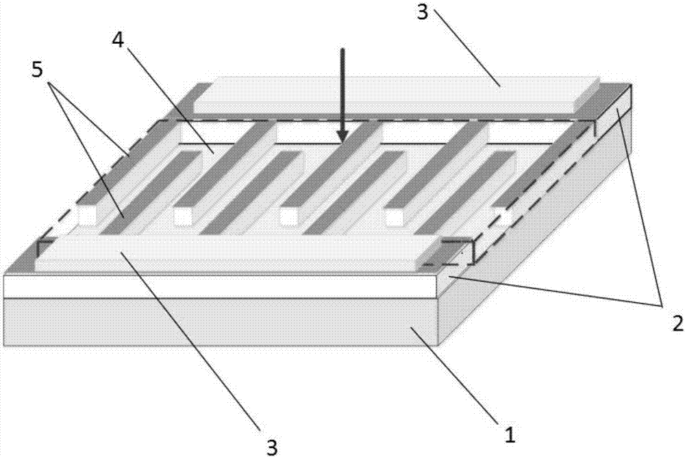
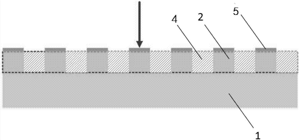
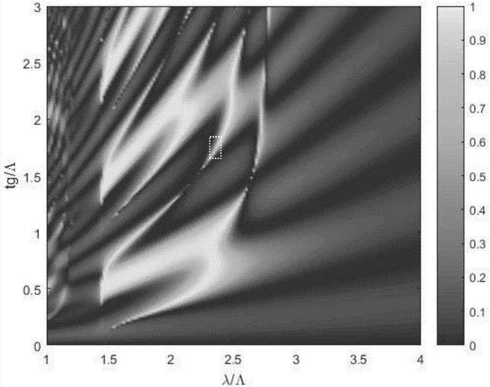
[0040] In this embodiment, the simulation parameters are set as follows: in this embodiment, the material of the substrate 1 is silicon dioxide, and the material of the grating 2 is silicon; the grating period Λ is 650 nm, the duty ratio is 0.5, and the grating thickness is 1100 nm; The refractive index of the substrate material is 3.48, the refractive index of the substrate material is 1.44, and the refractive index of the electro-optic material layer material n 0 (when the driving voltage is zero) is 1.60.

[0041] In this embodiment, TM polarized light is incident, and since the thickness of the transparent conductive layer 5 is very small, the influence of the thickness of the transparent conductive layer 5 can be ignored in the simulation process. In this embodiment, the strict coupled wave analysis method is used for simulation, and Matlab simulation software is used to draw the following image 3 Reflectance contour plot of the shown electro-optic tunable filter based ...

Embodiment 2

[0045] In this embodiment, the simulation parameters are set as follows: in this embodiment, the material of the substrate 1 is silicon dioxide, and the material of the grating 2 is silicon; the grating period Λ is 650 nm, the duty ratio is 0.5, and the grating thickness is 1100 nm; The refractive index of the substrate material is 3.48, the refractive index of the substrate material is 1.44, and the refractive index of the electro-optic material layer material is 1.65 (the driving voltage is not zero at this time); the electro-optic material selects the electro-optic coefficient r 33 300pm / V electro-optic polymer.

[0046] In this embodiment, TM polarized light is used for incident, and the simulation is carried out according to the strict coupled wave analysis method, and the following is obtained by using Matlab simulation software to draw Figure 5 The reflectance spectrum is shown, in which, the small picture in the upper right corner is an enlarged view of the reflectanc...

Embodiment 3

[0052] In this embodiment, the simulation parameters are set as follows: in this embodiment, the material of the substrate 1 is silicon dioxide, and the material of the grating 2 is silicon; the grating period Λ is 650 nm, the duty ratio is 0.5, and the grating thickness is 1100 nm; The refractive index of the substrate material is 3.48, the refractive index of the substrate material is 1.44, and the refractive index of the electro-optic material layer material is 1.70 (the driving voltage is not zero at this time); the electro-optic material selects the electro-optic coefficient r 33 300pm / V electro-optic polymer.

[0053] In this embodiment, TM polarized light is used for incident, and the simulation is carried out according to the strict coupled wave analysis method, and the following is obtained by using Matlab simulation software to draw Figure 6 The reflectance spectrum is shown, in which, the small picture in the upper right corner is an enlarged view of the reflectanc...


PUM

PropertyMeasurementUnit
electro-optic coefficientaaaaaaaaaa
wavelengthaaaaaaaaaa
electro-optic coefficientaaaaaaaaaa

Abstract

The invention discloses an electrooptical adjustable filter based on a sub-wavelength high-contrast grating and relates to the technical field of photoelectrons. The electrooptical adjustable filter comprises a substrate, an interdigital sub-wavelength grating, a transparent conduction layer and electrodes that are stacked sequentially from the bottom up, wherein an electrooptic material layer flush with the transparent conduction layer is arranged at an exposed part on the surface of the substrate; the two electrodes are connected with an external circuit to form an electric field between grating ridges; and a refractive index of a material of the interdigital sub-wavelength grating is much greater than those of materials of the substrate, the photoelectric material layer and the transparent conduction layer. The filter is reasonable in structural design, and can obtain high quality factor resonance and an adjustable filtration spectral range via reasonable selection of grating parameters, and tune filtration wavelength via voltage modulation; further, the refractive index of an electrooptic material is regulated based on an electric field effect; and compared with a mechanical adjustable filter, the tuning precision and tuning speed are greatly improved and increased. The filter is simple in structure, the materials are easy to obtain, and large-scale production and application are facilitated.

Description

technical field [0001] The invention belongs to the technical field of optoelectronics, and specifically relates to a filter capable of realizing the adjustable filtering function of the optical communication band through an external voltage. Background technique [0002] In today's digital age, optical communication technology is developing at an unimaginable speed, and wavelength division multiplexing (Wavelength division multiplexer, WDM) has greatly increased the capacity of optical communication systems. With the application of wavelength division multiplexing (WDM) technology, optical communication technology has developed rapidly. In the future, optical communication technology will develop in a more intelligent and efficient direction. As a key device in wavelength division multiplexing technology, tunable optical filters have received more and more attention and research. The tunable optical filter is a wavelength selection device, and its function is to select an ...

Claims


Application Information

Patent Timeline
Patent Type & Authority Applications(China)
IPC IPC(8): G02F1/03
CPCG02F1/0311
Inventor 李佳城张雅丽喻寅书刘爽刘永
Owner UNIV OF ELECTRONICS SCI & TECH OF CHINA
Why Eureka
Try Eureka