
DFB laser based on surface gating

A technology of DFB lasers and surface gratings, applied in lasers, semiconductor lasers, phonon exciters, etc., can solve the problems of complex etching process, large electrode loss, high cost, etc., achieve simple manufacturing process, reduce manufacturing cost, and improve reliability sexual effect

Active Publication Date: 2017-06-13
HUAZHONG UNIV OF SCI & TECH
View PDF5 Cites 16 Cited by
  • Summary
  • Abstract
  • Description
  • Claims
  • Application Information

AI Technical Summary

Problems solved by technology

The groove width here is only about 100nm. In order to realize such a deep-etched surface grating with narrow groove width experimentally, a relatively complicated etching process is usually required, so there are disadvantages of low yield and high cost.
[0005] In summary, existing commercial DFB lasers suffer from material regrowth issues, resulting in low yield and high cost
Existing surface grating lasers have the problem of small grating coupling coefficient or large electrode loss

Method used


Image

  • DFB laser based on surface gating
  • DFB laser based on surface gating
  • DFB laser based on surface gating

Examples


Embodiment Construction

[0030] The present invention will be described in detail below in conjunction with the accompanying drawings and specific embodiments.

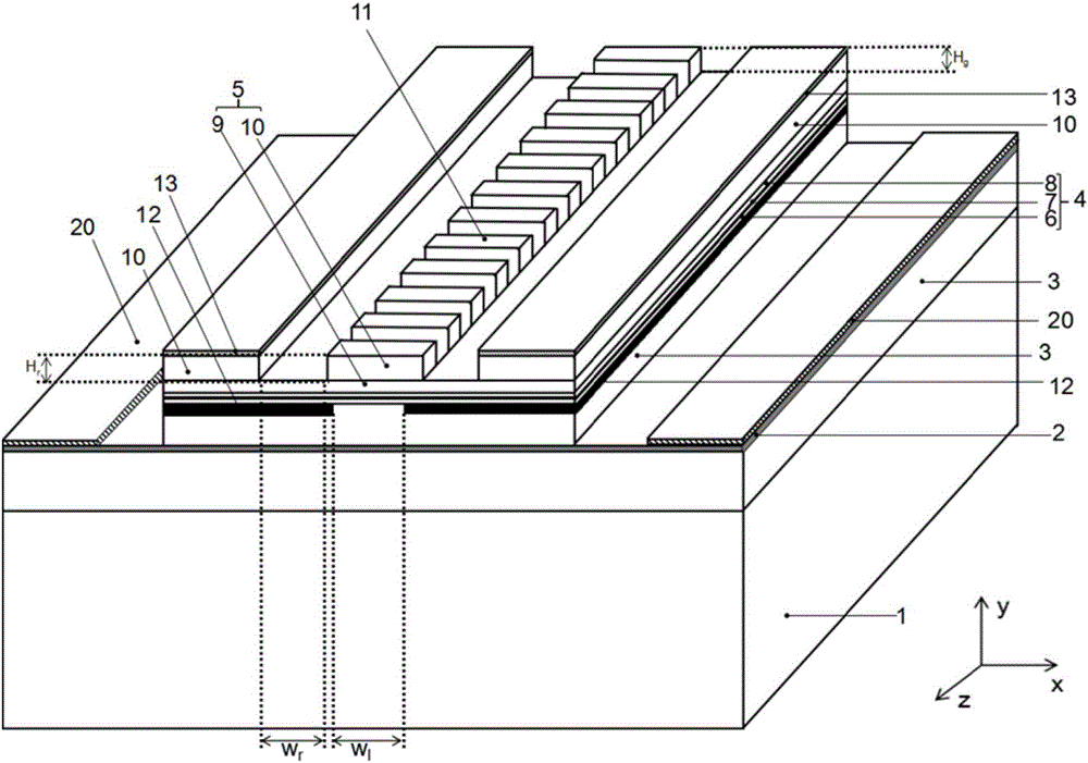
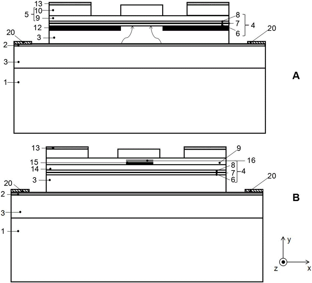
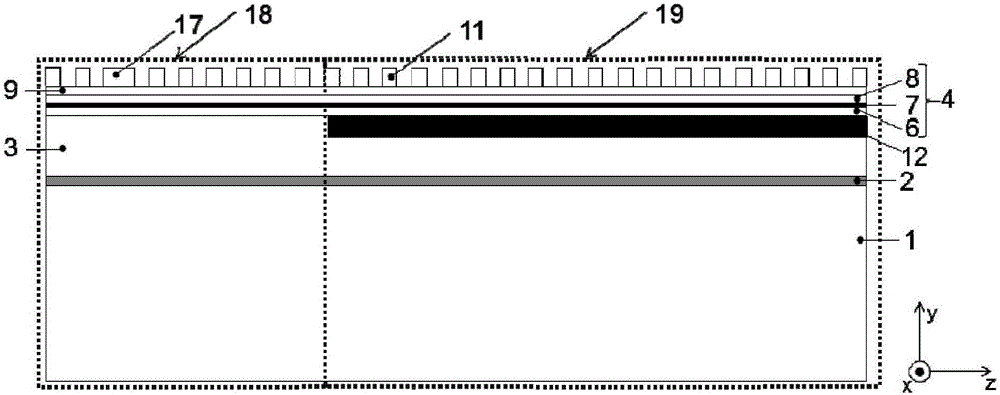
[0031] figure 1 is a schematic structural diagram of a surface grating-based DFB laser according to the present invention. The lateral, transverse and longitudinal directions of the laser are denoted as x, y and z directions, respectively, and all schematic diagrams use the same spatial coordinate system and labels. Such as figure 1 As shown, the layered structure of the semiconductor laser includes a substrate 1 , a lower waveguide capping layer 3 , an active layer 4 , and an upper waveguide capping layer 5 in a cross section from bottom to top. Among them, the lower waveguide cover layer 3 is P-type doped, the active layer 4 is not doped, the upper waveguide cover layer 5 is N-type doped, and the upper waveguide cover layer 5, the active layer 4 and the lower waveguide cover layer 3 jointly constitute N-i-P structure. From bottom to top...


PUM

PropertyMeasurementUnit
Thicknessaaaaaaaaaa
Coupling coefficientaaaaaaaaaa

Abstract

The invention discloses a DFB laser based on surface gating. The laser is of a ridge waveguide structure, and comprises a substrate, a lower waveguide cover layer, an active layer and an upper waveguide cover layer from the bottom up, wherein Bragg grating is etched in the surface of the ridge waveguide; the ridge area adopts high refractive material, so that the gating has a large coupling coefficient; no electrode is formed on the ridge waveguide, and the electrodes are positioned on two sides of the ridge waveguide; a groove is etched between the ridge waveguide and each of the electrodes on two sides; in the laser, the lower waveguide cover layer comprises one or more current limitation areas, or a buried tunnel junction is manufactured in the upper waveguide cover layer to limit current. According to the laser provided by the invention, secondary epitaxial growth of the material is not needed, the manufacturing technology is simple and convenient, and thus the manufacturing cost of the device is reduced, and the reliability of the device is improved. In addition, the laser provided by the invention can acquire the maximum coupling coefficient, so that the laser performance of low threshold and high-speed direct adjustment can be acquired in the case that the cavity length of the laser is extremely short.

Description

technical field [0001] The invention belongs to the technical field of semiconductor lasers, in particular to a DFB laser based on a surface grating. Background technique [0002] Distributed feedback (Distributed Feedback, DFB) laser (H.Kogelnik, C.V.Shank, "Coupled-wave theory of distributed feedback lasers," J.Appl.Phys., vol.43, pp.2327-2335, 1972.) has a narrow Line width, low chirp, tunable and other characteristics, so it has a wide range of applications in the fields of optical communication, optical storage and optical detection. The current mainstream commercial DFB lasers use buried first-order Bragg gratings to provide feedback. Usually, the Bragg gratings are etched in the upper waveguide cap layer very close to the active layer and the gratings are buried by regrowth. , so one or more material regrowth processes will be included in the production process. The re-growth process of this material complicates the fabrication of the laser, thereby reducing the yie...

Claims


Application Information

Patent Timeline
IPC IPC(8): H01S5/12H01S5/10
CPCH01S5/1028H01S5/12H01S5/22H01S5/2215H01S5/04257H01S5/04256H01S5/3095H01S5/2226H01S5/124H01S5/2063H01S5/0014H01S5/0287H01S5/0425H01S5/1206H01S5/125H01S5/3211
Inventor 陆巧银张鹏斐国伟华
Owner HUAZHONG UNIV OF SCI & TECH
Learn More