On-chip transformer Balun

An on-chip transformer and winding technology, which is applied in the direction of transformers, variable transformers, transformer/inductor components, etc., can solve the problems of high manufacturing process costs, reduce manufacturing process costs, increase the number of turns ratio, and reduce energy loss. Effect

Active Publication Date: 2017-10-24
SEMICON MFG INT (SHANGHAI) CORP +1
View PDF3 Cites 14 Cited by
  • Summary
  • Abstract
  • Description
  • Claims
  • Application Information

AI Technical Summary

Problems solved by technology

[0007] Another problem to be solved by the present invention is: the manufacturing process cost of the existing on-chip transformer balun is relatively high

Method used


Image

  • On-chip transformer Balun
  • On-chip transformer Balun
  • On-chip transformer Balun

Examples


no. 1 example

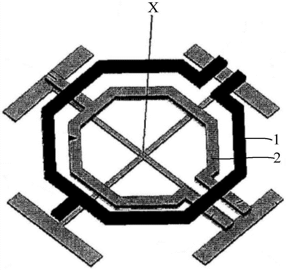
[0035] like figure 2 As shown, the on-chip transformer balun provided by this embodiment includes a primary coil 10 and a secondary coil 20 . Wherein, the primary coil 10 includes N turns of winding wire 11, N is greater than or equal to 2, the secondary coil 20 includes M turns of winding wire 21, and the turn ratio between the primary coil 10 and the secondary coil 20 of the on-chip transformer balun is N : M.

[0036] In this embodiment, take N equal to 2 and M equal to 1 as an example. The turn ratio between the primary coil 10 and the secondary coil 20 is 2:1. Compared with the existing on-chip transformer balun, the turn ratio of the on-chip transformer balun in this embodiment is improved.

[0037] Both the first terminal 12 and the second terminal 13 of the primary coil 10 are located on the outermost winding wire 11, so that there are N-1 overlapping regions Q in the N-turn winding wire 11 of the primary coil 10 (the double-dashed line ellipse in the figure locati...

no. 2 example

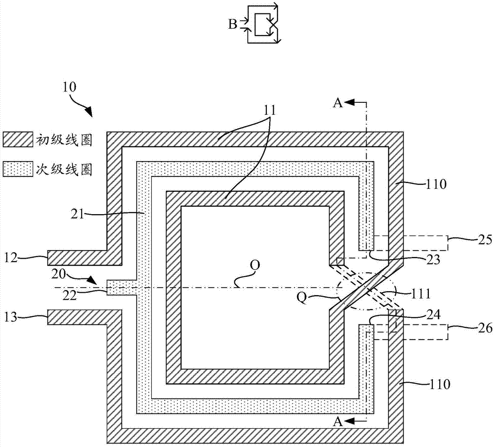
[0061] The difference between the second embodiment and the first embodiment lies in the number of turns of the primary coil and the configuration of the secondary coil.

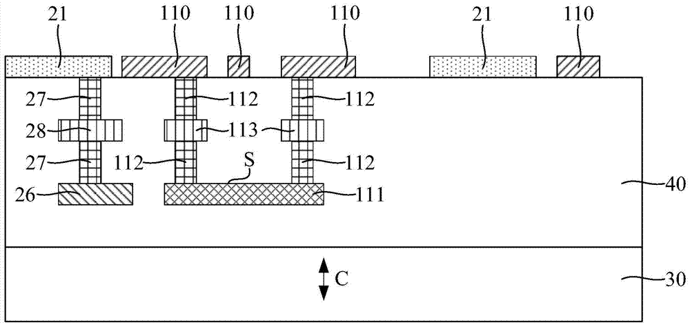
[0062] combine Figure 4 to Figure 5 As shown, in this embodiment, the number of turns N of the primary coil 10 is 3, the number of overlapping areas Q in the primary coil 10 is two, the number of first metal wires 110 in the primary coil 10 is five, and the connecting bridge The number of 111 is four. Two of the connection bridges 111 overlap at one of the overlapping regions Q, and the two of the connection bridges 111 are separated by a dielectric layer 40 . The other two connecting bridges 111 overlap at another overlapping area Q, and the other two connecting bridges 111 are separated by the dielectric layer 40 .

[0063] In a modified example of this embodiment, the number of first metal wires 110 in the primary coil 10 is four, and the number of connecting bridges 111 is three. Two of the connectio...

no. 3 example

[0068] The difference between the third embodiment and the first embodiment is that in the third embodiment, if Image 6 As shown, the on-chip transformer balun also includes a first capacitor 30 , a second capacitor 31 and a third capacitor 32 . Wherein, the two ends of the first capacitor 30 are respectively electrically connected to the first terminal 12 and the second terminal 13 of the primary coil 10, and the two ends of the second capacitor 31 are respectively electrically connected to the third terminal 23 and the center tap 22 of the secondary coil 20. The two ends of the third capacitor 32 are electrically connected to the fourth terminal 24 of the secondary coil 20 and the center tap 22 respectively.

[0069] The first capacitor 30 resonates with the primary coil 10, and the second capacitor 31 and the third capacitor 32 resonate with the secondary coil 20. By adjusting the capacitance values ​​of the first capacitor 30, the second capacitor 31 and the third capacit...


PUM

PropertyMeasurementUnit
thicknessaaaaaaaaaa

Abstract

An on-chip transformer Balun comprises a primary coil and a secondary coil, wherein the turns of the primary coil is N, a first terminal and a second terminal of the primary coil are arranged on a winding at the outermost turns so that (N-1) lamination regions exist in the winding of the primary coil, the primary coil comprises a plurality of first metal lines and a plurality of connection bridges which are arranged in a staggered way along a winding direction, the first metal lines are arranged on the same plane, the connection bridges are arranged below the plane, the connection bridges are electrically connected with the first metal lines at the lamination regions, upper surfaces of the connection bridges are covered by a dielectric layer below the plane, N is more than or equal to 2, the secondary coil with M turns is arranged on the plane, and a winding of the secondary coil is arranged between two adjacent turns of windings of the primary coil. The on-chip transformer Balun disclosed by the scheme is relatively large in coupling coefficient and small in energy loss, the turn numbers of the primary coil and the secondary coil are relatively large, and the manufacturing process is low in cost.

Description

technical field [0001] The invention relates to the technical field of on-chip passive devices, in particular to an on-chip transformer balon. Background technique [0002] Common baluns include high-frequency open circuit, offset and transformer. Among them: the high-frequency open-circuit balun has a narrow working bandwidth; the offset balun has a wide frequency band, but it is limited by the magnetic saturation of the magnetic ring when using high power; and the on-chip transformer balun mainly realizes balanced-unbalanced conversion through a high-frequency transformer. [0003] like figure 1 As shown, an existing on-chip transformer balun includes a primary coil 1 and a secondary coil 2. In the axial direction X of the primary coil 1 and the secondary coil 2, the primary coil 1 and the secondary coil 2 are arranged at intervals, and between the two are separated by a dielectric layer (not shown). [0004] The disadvantage of the existing on-chip transformer balun is...

Claims


Application Information

Patent Timeline
Patent Type & Authority Applications(China)
IPC IPC(8): H01F27/28H01F29/00
CPCH01F27/2871H01F29/00
Inventor 贾海珑刘文华
Owner SEMICON MFG INT (SHANGHAI) CORP
Why Eureka
Try Eureka