Metallic mold for optical element and optical element

a technology of optical elements and molds, which is applied in the direction of dough shaping, manufacturing tools, food shaping, etc., can solve the problems of poor machinability of raw materials, delicate dispersion of optical surface transfer surfaces, so as to improve the dimension accuracy of optical elements and excellent cutting properties

Inactive Publication Date: 2009-02-10
KONICA MINOLTA OPTO
View PDF5 Cites 32 Cited by
  • Summary
  • Abstract
  • Description
  • Claims
  • Application Information

AI Technical Summary

Benefits of technology

[0018]In view of such a problem of conventional technology, the present invention is attained and the object of the present invention is to provide a metallic mold for optical element which is excellent for cutting property and which can increase the dimension accuracy of the optical element, and the optical element molded thereby.
[0024]wherein the film layer is a film layer formed by an amorphous alloy having a supercooled liquid state containing 20 mol % or more of at least one atom of Pt, Ir, Au, Pd, Ru, Rh, Fe, Co, Ni, Zr, Al, Ti, Cu, W, Mo, Cr, B, and P and the transferring surface maintains the surface roughness after the transferring surface is heated to a temperature which is higher 50° C. higher than the glass transition temperature (Tg) of the material of the optical element formed by the transferring surface and lower than the glass transition temperature of the amorphous alloy.

Problems solved by technology

However, on the other hand, problems are generated in which: the mechanical processing and chemical plating processing are mixed in the manufacturing process and it is vexatiously complicated, and a long period of delivery is necessary; the manufacturing of blank (primary processed goods) is necessary, considering the thickness of plating layer; the plating processing is not always stable, and due to a deviation of composition of the blank or a soiled condition, the adhesion strength of the plating layer is dispersed, or a pinhole-like defect which is called a pit, is generated; and because the creation of the optical surface transfer surface is necessary in the thickness of plating layer, there is a case where there is not any margin in the plating thickness when the optical surface transfer surface is re-worked, and the processing can not be conducted.
Further, according to the conventional technology, it is necessary that the optical surface transfer surface is largely cutting processed by a diamond tool, however, in such a case, the influence such as a condition of a cutting edge of the tool or processing condition, a change of processing environmental temperature is exerted, and there is also a problem that the shape of the optical surface transfer surface finished after cutting processing, is delicately dispersed.
This processing dispersion of the optical surface transfer surface is due to the poorness of the machinability of the raw material.
In general, the optical surface shape error of about 100 nm is generated, and even in the case where processing is conducted very carefully, the shape error of about 50 nm is remained.
This is a limit of processing accuracy when a large amount of optical surface transfer surfaces of the same shape are created.
Such an optical element can be produced in a large amount and effectively by molding, however, it is a very important problem, at the time of molding, how high-accurately and effectively minute diffraction grooves on the optical surface of the optical element are manufactured by the metallic mold for optical element.
Further, it is necessary that the feed speed of the tool is made slow in order also to prevent the deterioration of the surface roughness of the optical surface by the cutter mark of the small cutting edge, and the optical surface transfer surface processing time per one time also becomes long.
As a result, in the cutting processing of the metallic mold for molding the optical element having the diffraction groove, because the cutting length is increased, wearing of the cutting edge of the tool is increased, and the tool change becomes often.
That is, when the optical surface transfer surface having minute shape is processed by the conventional diamond cutting, because the life of the tool is very shortened and a time period for processing one optical surface transfer surface is also increased, it is necessary that the tool is changed often, therefore, the processing efficiency is very much lowered, and the productivity of the metallic mold for optical element is lowered, resulting in the rapid increase of the cost.
However, relating to the protrusion (or recess) of the equivalent refraction area or resonance area as described above, because it is necessary that protrusions (or recesses) are formed at the interval of several-tens or several-hundreds nm, it is very difficult by the mechanical processing including the cutting processing.
However, because the hardness of these materials are hard materials of Hv 1000-3000 in Vickers hardness, when compared to the electroless nickel plating (about Hv 500-600), which is easily cut, they are very difficult in processing, it is difficult to increase the processing shape accuracy or the mirror property of the metallic mold molded transfer surface, or the processing time period more than four times than that of the plating materials is also necessary.
However, in the Patent Document 1, a specific adhering amount or temperature range is not regulated, and by the content written in the Patent Document 1, it is difficult that the metallic mold for the optical element is actually manufactured.

Method used


Image

  • Metallic mold for optical element and optical element
  • Metallic mold for optical element and optical element
  • Metallic mold for optical element and optical element

Examples


example

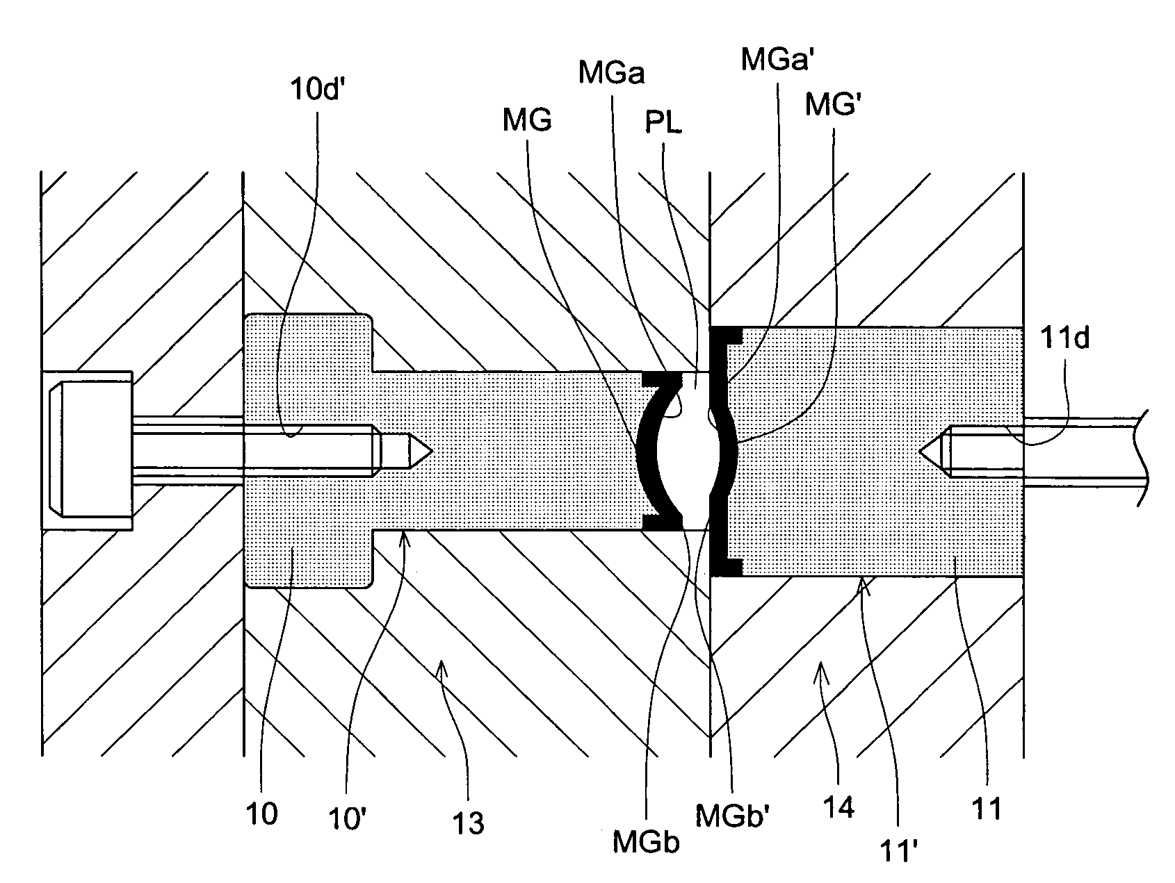
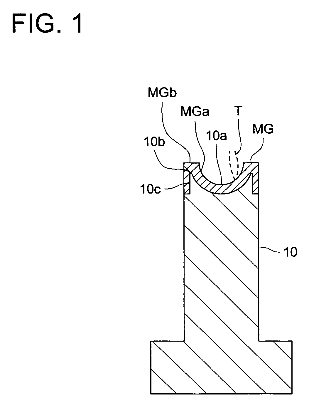
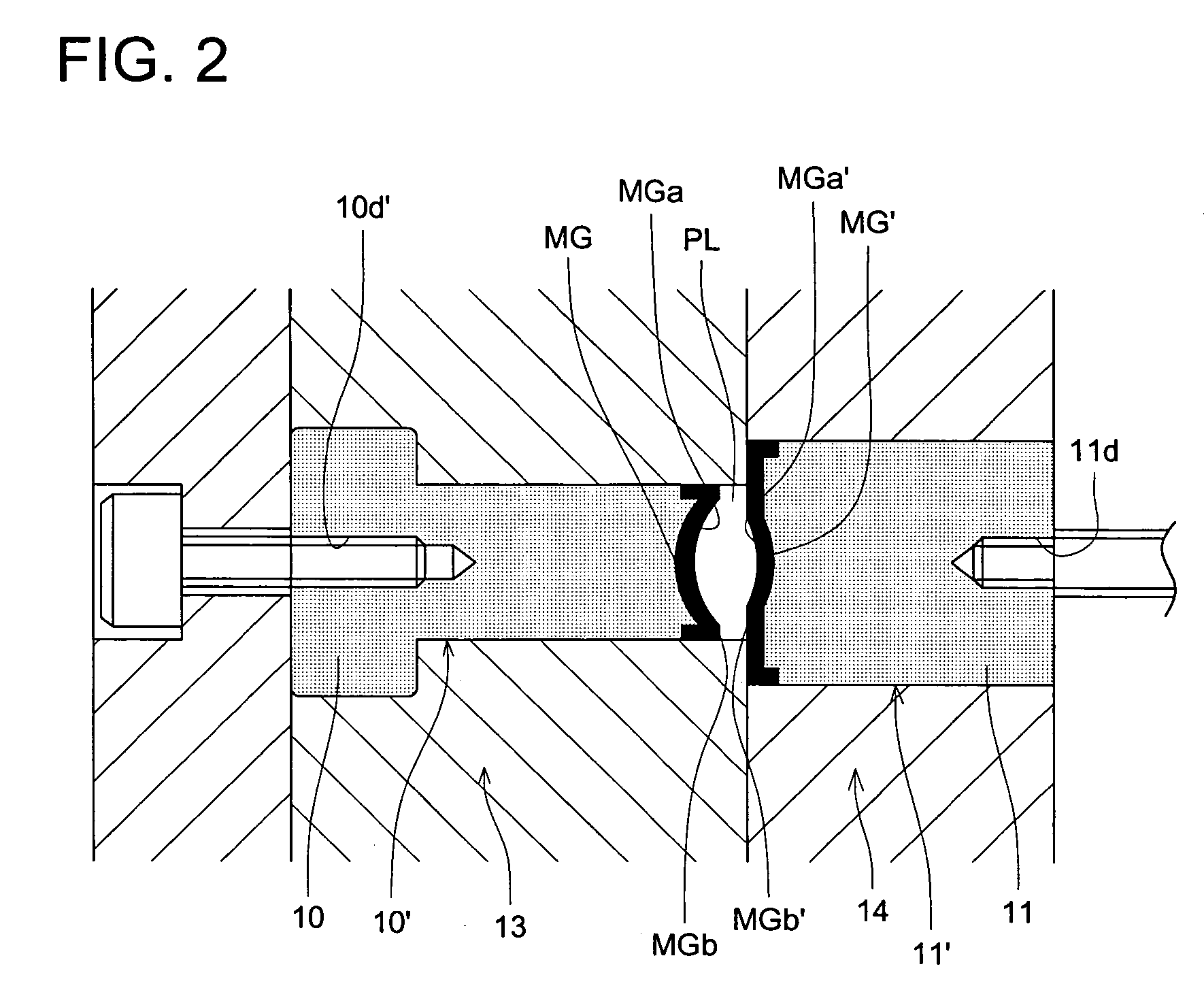
[0093]The present inventor manufactured, in the above-described manner, the metallic mold for the optical element by using Pd76Cu6Si18 series metal glass as the amorphous material of the molding transfer surface. When the surface roughness of the molding transfer surface at the time of finishing processing completion is measured, it is Ra 10 nm, and the shape error is within ±50 nm. By using this metallic mold for the optical element, the plastic lens raw material whose glass transition temperature is Tg 200° C., was molded under the molding condition of the molding resin temperature 250° C., and pressure 800 kg / cm2. Even when the molding of 2000shot is conducted, the optical elements whose accuracy is good, are stably obtained, further, the surface roughness on the molding transfer surface is Ra 10 nm, and there is no change, and particularly, the change of the shape was also not seen. For the metallic mold for the optical element of the present invention, the same effect can be ex...


PUM

PropertyMeasurementUnit
thicknessaaaaaaaaaa
surface roughness Raaaaaaaaaaa
glass transition temperatureaaaaaaaaaa

Abstract

A molding die for forming an optical element, comprises a base body; a film layer formed on the base body and having a thickness of 0.01 to 500 μm; and a transferring surface formed on a surface of the film layer by a predetermined process and having a surface roughness Ra of 0.1 to 50 nm. The film layer is formed by an amorphous alloy having a supercooled liquid state containing 20 mol % or more of at least one atom of Pt, Ir, Au, Pd, Ru, Rh, Fe, Co, Ni, Zr, Al, Ti, Cu, W, Mo, Cr, B, and P and the transferring surface maintains the surface roughness after the transferring surface is heated to a temperature which is higher 50° C. higher than the glass transition temperature (Tg) of the optical element formed by the transferring surface and lower than the glass transition temperature of the amorphous alloy.

Description

[0001]This application is based on Japanese Patent Application No. 2004-114853 filed on Apr. 9, 2004, in Japanese Patent Office, the entire content of which is hereby incorporated by reference.BACKGROUND OF THE INVENTION[0002]The present invention relates to a metallic mold for an optical element, which is manufactured by using the amorphous alloy having a supercooled liquid state, and to the optical element.[0003]According to the manufacturing method of a molding die of a plastic optical element which is conventionally generally conducted, a blank (primary product) is manufactured by, for example, steel or stainless steel, and an alloy of an amorphous-like nickel and phosphorous is filmed in the thickness of about 100 μm by a chemical plating, which is called electroless plating, on it, and this plating layer is cutting processed by a diamond tool of an ultra-precise processing machine, and a highly accurate optical surface transfer surface for molding the optical surface of the op...

Claims


Application Information

Patent Timeline
Patent Type & Authority Patents(United States)
IPC IPC(8): B29C33/00B29C43/32B29C33/38B29D11/00C03B11/00
CPCB29D11/00413
Inventor YUASA, SEIJIHOSOE, SHIGERUATARASHI, YUICHI
Owner KONICA MINOLTA OPTO
Why Eureka
Try Eureka