Circuit and method for gain error correction in ADC

Active Publication Date: 2009-02-24
TEXAS INSTR INC
View PDF4 Cites 38 Cited by
  • Summary
  • Abstract
  • Description
  • Claims
  • Application Information

AI Technical Summary

Benefits of technology

[0019]It is an object of the invention to provide an ADC which corrects its ADC transfer characteristic for gain error without increasing the amount of

Problems solved by technology

However, the known analog techniques for correcting ADC gain error require increased amounts of integrated circuit die area, and they typically require use of costly laser trimming techniques.
Furthermore, the gain correction accuracy which can be achieved using analog ADC gain error correction techniques is less than can be achieved using digital ADC gain error correction techniques.
A problem with the above described prior art technique is that implementing a digital multiplier is always expensive because it requires complex circuitry and a large amount of integrated circuit die area, and also because it requires a large amount of quiescent current and hence a large amount of power dissipation.
The above described prior art technique also is very time-consuming, because the analog-to-digital conversion must be performed first, and then the slow digital multiplication of the ADC conversion result must be multiplied, bit by bit, by the digital error correction coefficient, which adds a substantial amount to the time required for the basic ADC conversion process in order to obtain a

Method used


Image

  • Circuit and method for gain error correction in ADC
  • Circuit and method for gain error correction in ADC
  • Circuit and method for gain error correction in ADC

Examples


Embodiment Construction

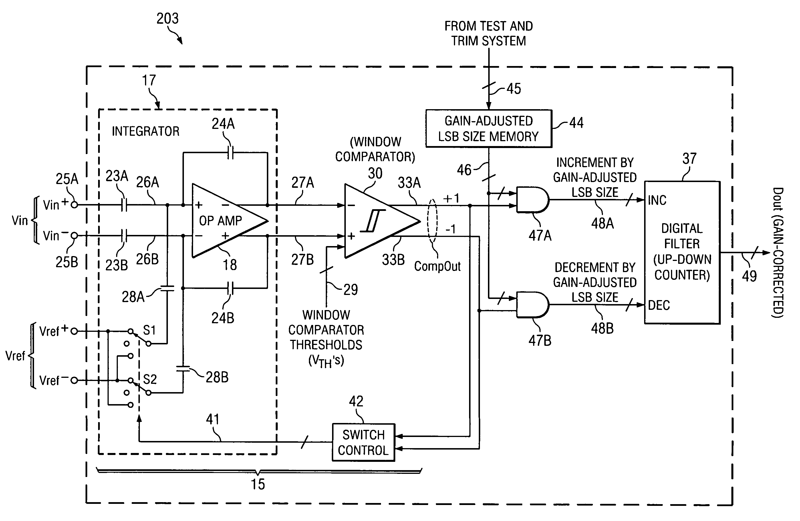
[0042]Referring to FIG. 3, integrated circuit delta-sigma ADC chip 20B includes integrator 17, the (−) output 27A of which is coupled to the (−) input of a window comparator 30. The (+) output 27B of integrator 17 is coupled to the (+) input of window comparator 30. Window comparator 30 may be composed of two or more conventional comparators which may receive various thresholds voltages VTH on the conductors of window comparator threshold bus 29, respectively. (By way of definition, it should be understood that if a conventional comparator receives a differential input signal, it may be considered to have a zero threshold voltage. The term “threshold voltage” as used herein is intended to encompass a threshold voltage applied to one input of a 2-input comparator the other input of which receives an input signal voltage that is to be compared with the threshold voltage, and is intended to also encompass a zero threshold voltage of a comparator which receives a differential input sign...


PUM


Abstract

Gain errors are corrected in an ADC chip including an integrator (17), a comparator (30), and a digital filter (37) by storing a gain-adjusted LSB size based on measured gain error in a memory (44). The gain-adjusted LSB size is applied to the digital filter to cause gain-adjusted LSB size values to be added to or subtracted from accumulated content of the digital filter in accordance with a first or second state, respectively, of the comparator (30) during each cycle of the ADC. The final accumulated content after all required cycles of the ADC is a gain-corrected digital output signal (Dout(gain-corrected)).

Description

BACKGROUND OF THE INVENTION[0001]The present invention relates generally to integrated circuit ADCs (analog to digital converters), and particularly to ADC circuits and methods for correcting the gain of an ADC with minimum circuit complexity, a minimum amount of integrated circuit chip area, and a minimum amount of time required in addition to the basic ADC conversion time in order to accomplish the gain error correction.[0002]Every ADC has gain error. There are two basic ways to correct the ADC gain error, namely analog correction and digital correction. One analog gain error correction technique is trimming of the reference voltage. That controls the transfer function of the converter so as to achieve whatever correction is needed for its gain. Another analog ADC gain correction technique is scaling the ratios of the sampling capacitors of the integration stage of the ADC. However, the known analog techniques for correcting ADC gain error require increased amounts of integrated c...

Claims


Application Information

Patent Timeline
IPC IPC(8): H03M1/06
CPCH03M1/1019H03M3/382H03M1/40H03M1/46H03M3/43H03M3/456
Inventor TRIFONOV, DIMITAR T.DOORENBOS, JERRY L.
Owner TEXAS INSTR INC
Why Eureka
Try Eureka