Transparent electrode for semiconductor light-emitting device
a technology of light-emitting devices and transparent electrodes, which is applied in the direction of semiconductor devices, basic electric elements, electrical appliances, etc., can solve the problems of high specific resistance of type gan compound semiconductors, increase in contact resistance, and rise of forward voltage (vsub>f/sub>), and achieve excellent ohmic contact, reduce resistance magnitude, and fast adhesion
- Summary
- Abstract
- Description
- Claims
- Application Information
AI Technical Summary
Benefits of technology
Problems solved by technology
Method used
Image
Examples
example 1
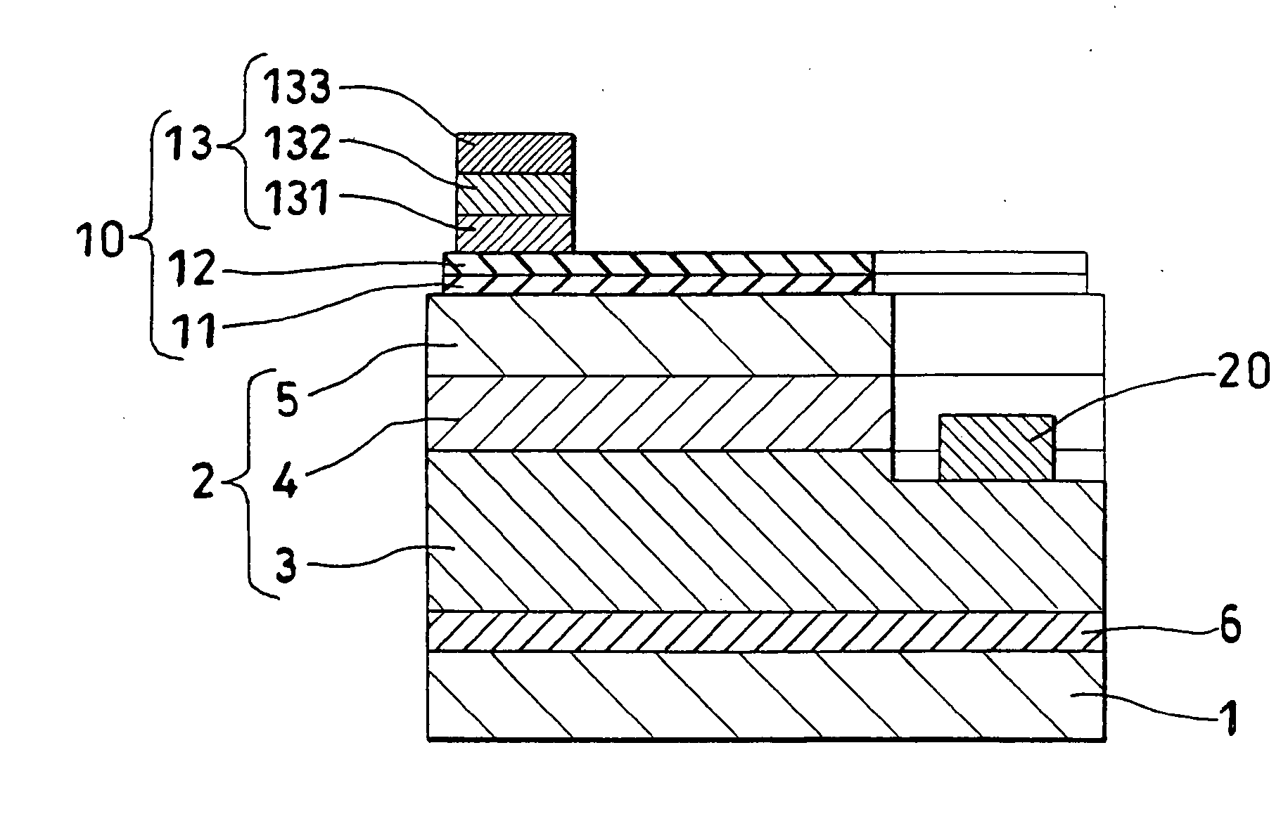
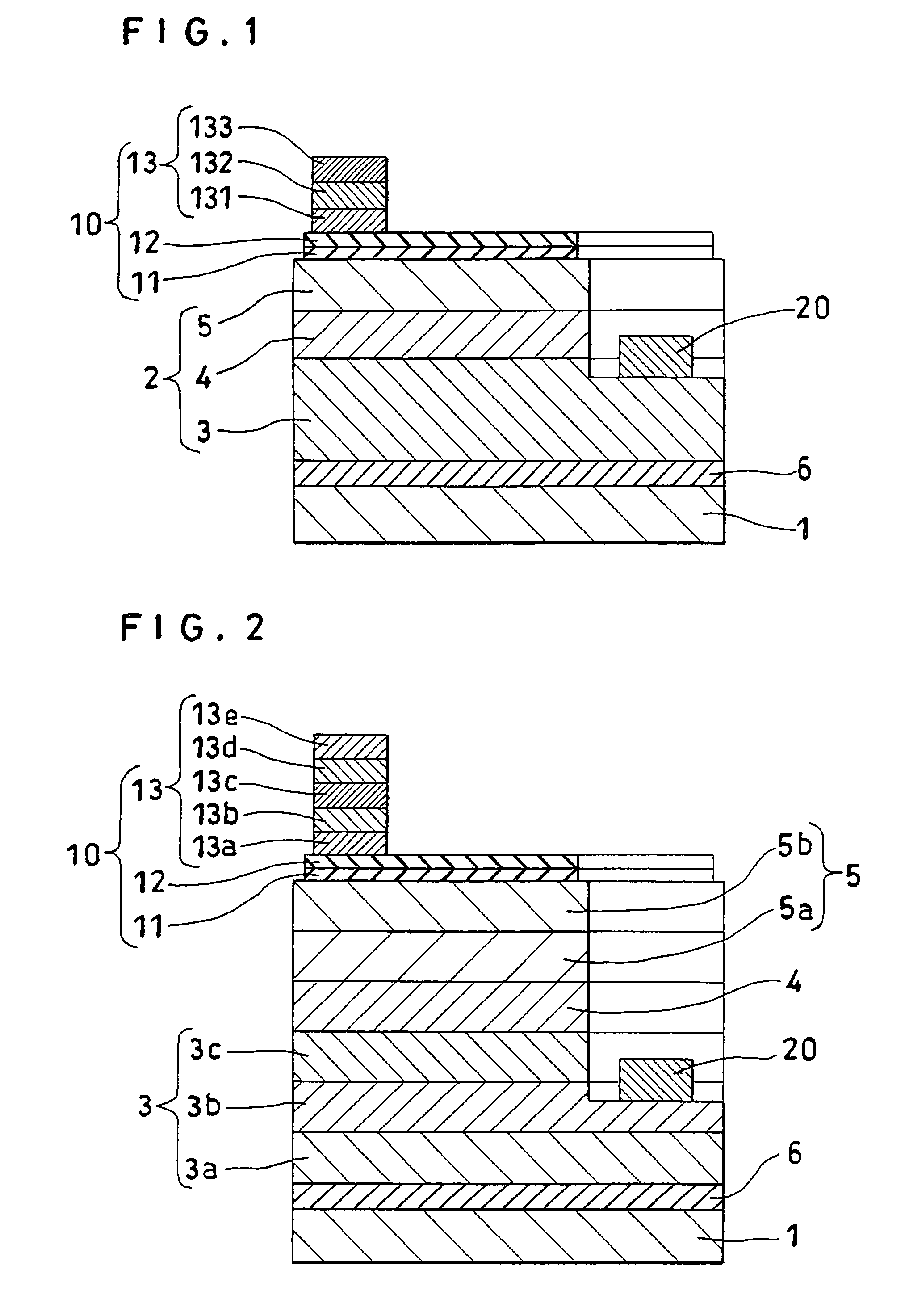
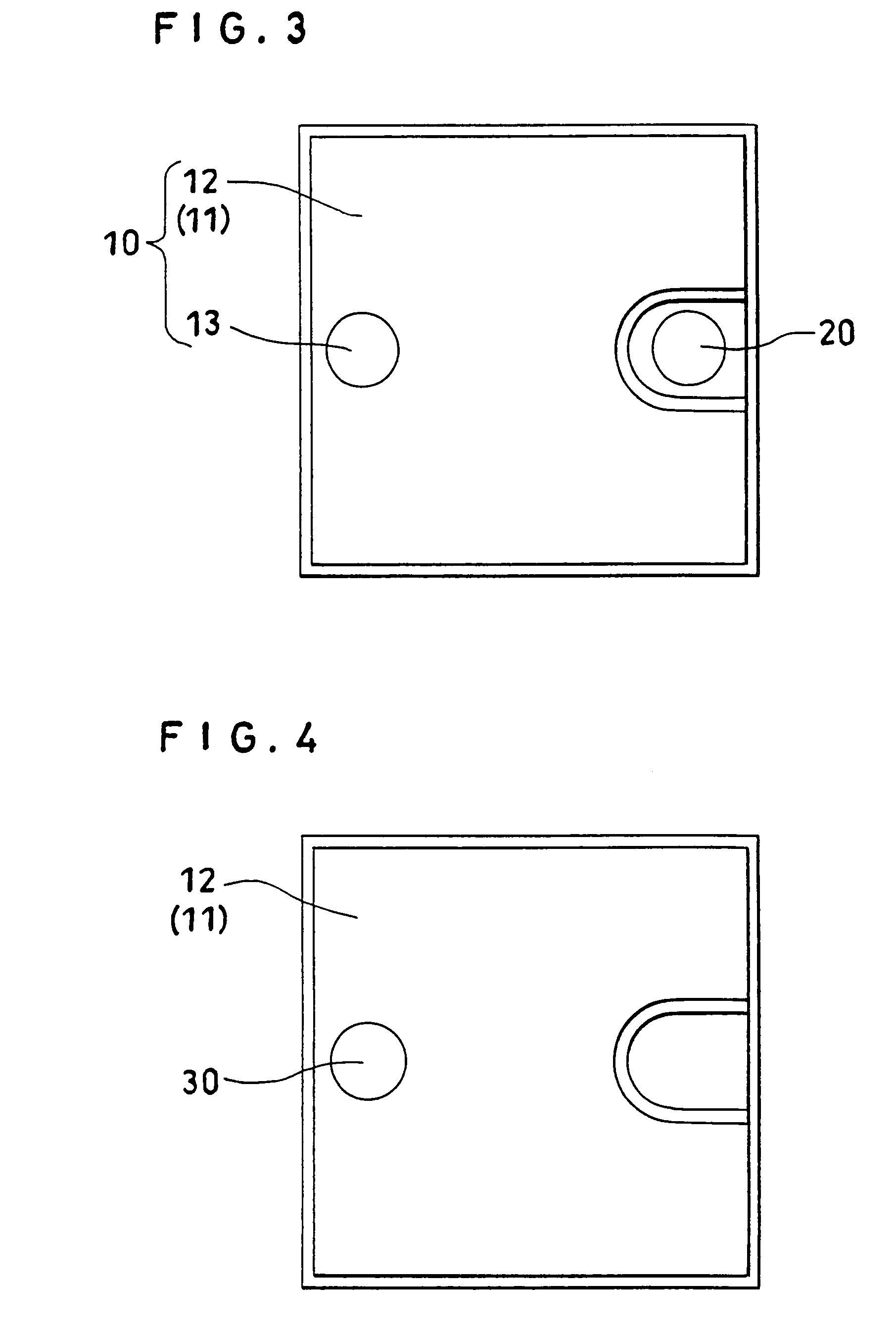
[0059]FIG. 2 is a schematic view illustrating the cross section of a gallium nitride-based compound semiconductor light-emitting device fabricated in this example and FIG. 3 is a schematic view illustrating the plan view thereof. On a substrate 1 made of sapphire, an under layer 3a made of undoped GaN and measuring 8 μm in thickness, an Si-doped n-type GaN contact layer 3b measuring 2 μm in thickness, an n-type In0.1Ga0.9N cladding layer 3c measuring 250 nm in thickness, a Si-doped GaN barrier layer measuring 16 nm and an In0.2Ga0.8N well layer measuring 1.5 nm in thickness were stacked through a buffer layer 6 made of AlN up to five repetitions. Finally, a positive electrode 10 of this invention formed of a bonding pad layer 13 of a five-layer structure consisting of a Pt contact metal layer 11 measuring 1.5 nm in thickness, an Au current diffusion layer 12 measuring 5 nm in thickness, an Au layer 13a measuring 50 nm in thickness, a Ti layer 13b measuring 20 nm in thickness, an Al ...
example 2
[0073]In Example 2, an electrode was formed in the following structure with a substrate having the same stacked structure as in Example 1.
[0074]Specifically, a positive electrode 10 of this invention was formed of a bonding pad 13 in a five-layer structure consisting of a Pt contact metal layer 11 measuring 1.5 nm in thickness, an ITO current diffusion layer 12 measuring 100 nm in thickness and a Cr layer 13a measuring 50 nm in thickness, a Ti layer 13b measuring 20 nm in thickness, an Al layer 13c measuring 10 nm in thickness, a Ti layer 13d measuring 100 nm in thickness and an Au layer 13e measuring 200 nm in thickness. In the five layers which formed the bonding pad, the Cr layer 13a measuring 50 nm in thickness constituted a first layer, the Ti layer 13b measuring 20 nm in thickness a second layer, the Al layer 13c measuring 10 nm in thickness a barrier layer, the Ti layer 13d measuring 100 nm in thickness a layer for preventing Al and Au from being alloyed, and the Au layer 13e...
PUM
 Abstract
Description
Claims
Application Information


