Low-temperature metal-induced crystallization of silicon-germanium films

a technology of silicongermanium and low temperature, applied in the field of low temperature crystallization method of silicongermanium film, can solve the problems of low thermal tolerance, adverse effects of high temperature required to crystallize deposited semiconductor materials such as silicon and silicon-germanium alloys, and inability to use desirable conductive materials

Active Publication Date: 2009-03-10
SANDISK TECH LLC
View PDF6 Cites 51 Cited by
  • Summary
  • Abstract
  • Description
  • Claims
  • Application Information

AI Technical Summary

Problems solved by technology

The relatively high temperature required to crystallize deposited semiconductor materials such as silicon and silicon-germanium alloys can have adverse effects on semiconductor devices.
High temperatures can lead to unwanted diffusion of dopants, can cause peeling due to differential expansion and contraction of unlike materials during thermal cycles, and can prohibit the use of desirable conductive materials like aluminum which have low thermal tolerance.
These disadvantages are particularly acute in monolithic three dimensional memory arrays, in which a memory level formed above a substrate will be exposed to the temperatures required to form additional memory levels stacked above it.

Method used


Image

  • Low-temperature metal-induced crystallization of silicon-germanium films
  • Low-temperature metal-induced crystallization of silicon-germanium films
  • Low-temperature metal-induced crystallization of silicon-germanium films

Examples


Embodiment Construction

[0004]The present invention is defined by the following claims, and nothing in this section should be taken as a limitation on those claims. In general, the invention is directed to crystallization of a deposited silicon-germanium alloy film.

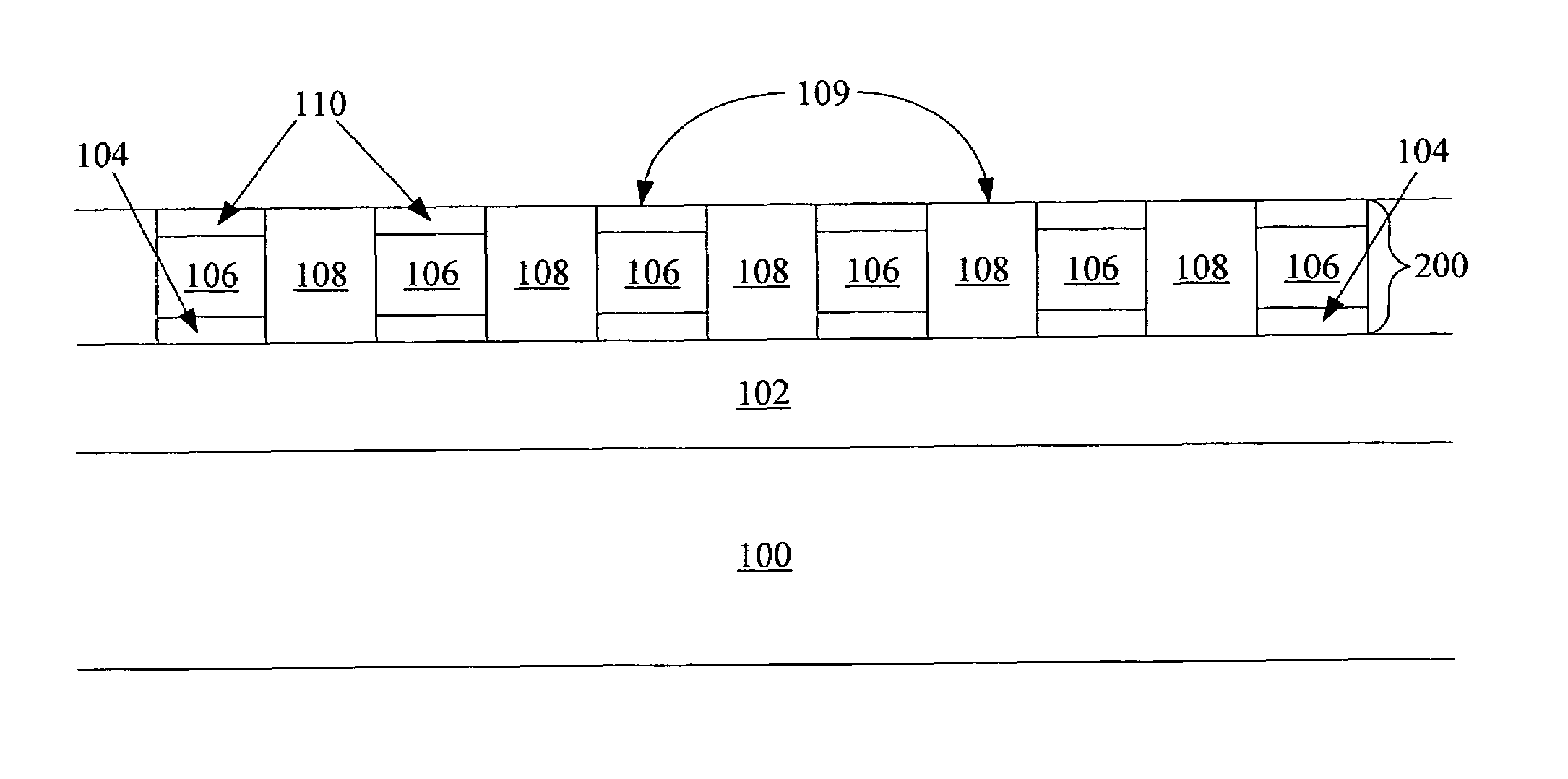
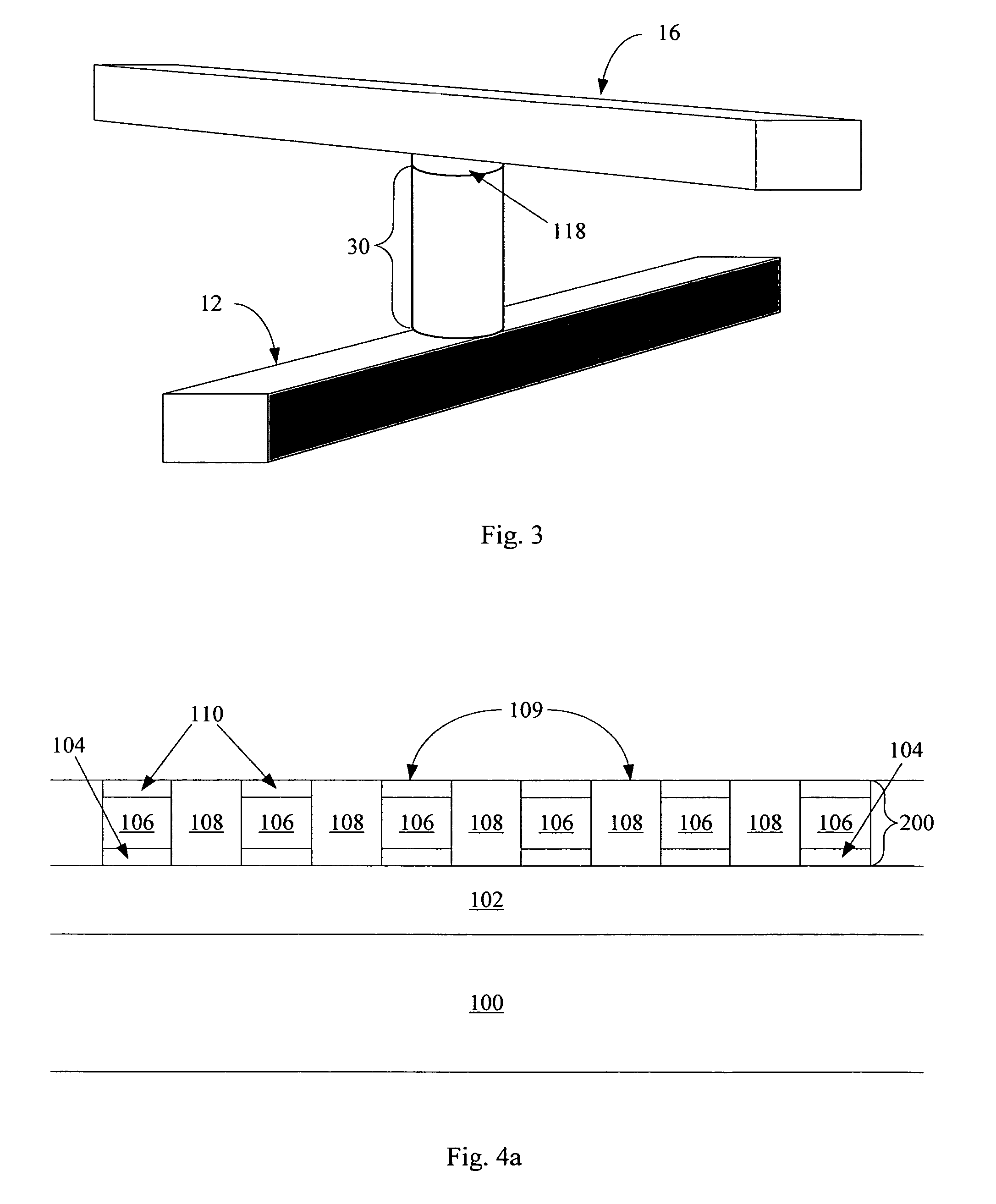
[0005]A first aspect of the invention provides for a method for crystallizing a semiconductor film, the method comprising: depositing a film of a silicon-germanium alloy at a temperature below about 490 degrees C.; depositing a layer of a metal catalyst selected from the group consisting of nickel, cobalt, ruthenium, and aluminum, the metal catalyst in contact with the silicon-germanium film; and crystallizing the silicon-germanium alloy film at a temperature below about 490 degrees C.

[0006]A preferred embodiment of the present invention provides for a method for forming a first memory level comprising a plurality of first memory cells, the method comprising: depositing a film of a silicon-gernanium alloy at a temperature below about 490 degrees...


PUM

PropertyMeasurementUnit
thicknessaaaaaaaaaa
thicknessaaaaaaaaaa
thicknessaaaaaaaaaa

Abstract

The present invention provides for a low-temperature method to crystallize a silicon-germanium film. Metal-induced crystallization of a deposited silicon film can serve to reduce the temperature required to crystallize the film. Increasing germanium content in a silicon-germanium alloy further decreases crystallization temperature. By using metal-induced crystallization to crystallize a deposited silicon-germanium film, temperature can be reduced substantially. In preferred embodiments, for example in a monolithic three dimensional array of stacked memory levels, reduced temperature allows the use of aluminum metallization. In some embodiments, use of metal-induced crystallization in a vertically oriented silicon-germanium diode having conductive contacts at the top and bottom end is be particularly advantageous, as increased solubility of the metal catalyst in the contact material will reduce the risk of metal contamination of the diode.

Description

BACKGROUND OF THE INVENTION[0001]The invention relates to a low-temperature method to crystallize a silicon-germanium film.[0002]The relatively high temperature required to crystallize deposited semiconductor materials such as silicon and silicon-germanium alloys can have adverse effects on semiconductor devices. High temperatures can lead to unwanted diffusion of dopants, can cause peeling due to differential expansion and contraction of unlike materials during thermal cycles, and can prohibit the use of desirable conductive materials like aluminum which have low thermal tolerance. These disadvantages are particularly acute in monolithic three dimensional memory arrays, in which a memory level formed above a substrate will be exposed to the temperatures required to form additional memory levels stacked above it.[0003]There is advantage, therefore, in lowering the temperature required to crystallize deposited semiconductor material.SUMMARY OF THE PREFERRED EMBODIMENTS[0004]The prese...

Claims


Application Information

Patent Timeline
Patent Type & Authority Patents(United States)
IPC IPC(8): H01L21/20
CPCC30B1/00C30B29/52H01L21/02532H01L21/02672H01L27/1021H01L29/66136H01L23/5252H01L2924/0002Y10S438/933Y10S148/059H01L2924/00
Inventor HERNER, S. BRAD
Owner SANDISK TECH LLC
Why Eureka
Try Eureka