Device manufacturing process utilizing a double patterning process

a technology of patterning and device manufacturing, applied in the direction of photomechanical treatment, instruments, electrical equipment, etc., can solve the problems of 40 watt output power, slow method to reach the market, impractical production use,

Inactive Publication Date: 2008-08-21
FUJIFILM ELECTRONICS MATERIALS US
View PDF12 Cites 162 Cited by
  • Summary
  • Abstract
  • Description
  • Claims
  • Application Information

AI Technical Summary

Problems solved by technology

This method has been slow to reach the market due to the immaturity of photoresist systems, and the source limitations associated with the EUV tool.
The current systems are only capable to producing 20-40 Watts of output power, which impractical for production use.
The timing required to resolve the current issues related to this technology will not likely be available for next generatio

Method used


Image

  • Device manufacturing process utilizing a double patterning process
  • Device manufacturing process utilizing a double patterning process
  • Device manufacturing process utilizing a double patterning process

Examples


formulation example 1

Fixer Formulation Example 1

Image Fixing Solution

[0203]An image fixing solution was prepared consisting of 4 parts by weight of hexamethylenediamine, 69 parts by weight of decane, and 27 parts by weight of 2-octanol. The components were mixed in an amber glass bottle, which was rolled for 24 hours during the mixing process.

process example 1

Lithographic Process Example 1

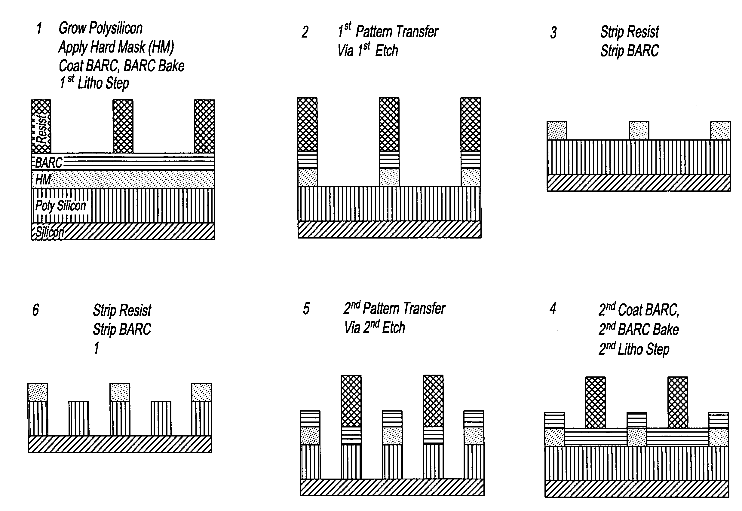
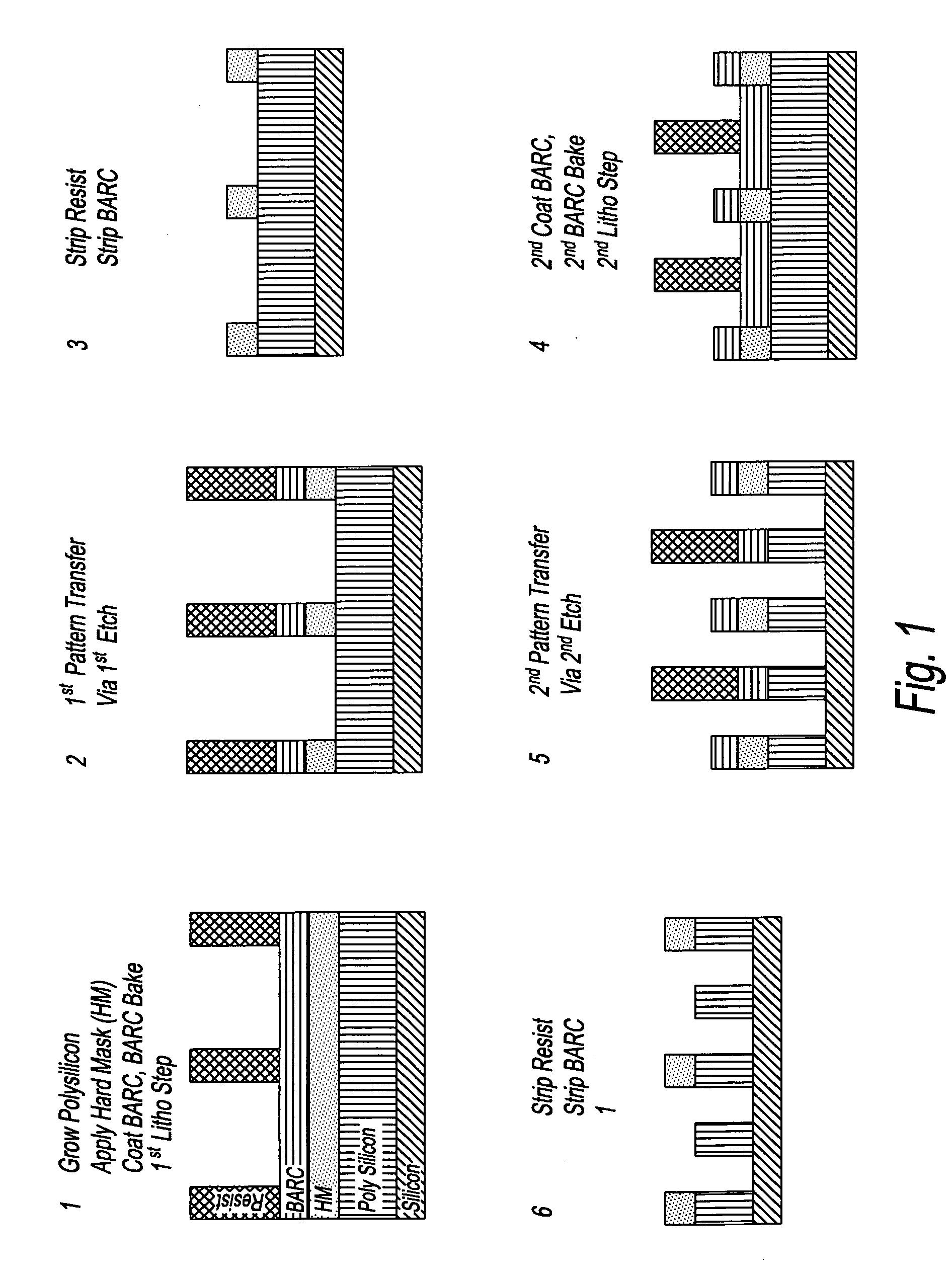
[0204]TIS 248UL-01-50 underlayer available from FUJIFILM Electronic Materials U.S.A., Inc., was applied to a 200 mm silicon wafer and spun coated using a DNS 80B coating track, to achieve a film thickness on 500 nm after baking for 200° C. for 70 seconds, using an inline bake plate configured within the DNS 80B. TIS 248IL-01-23 imaging layer photoresist, a chemically amplified, silicon and anhydride containing resist available from FUJIFILM Electronic Materials U.S.A., Inc., was applied onto the underlayer, using the DNS 80B coating track, to achieve a film thickness of 239 nm after baking for 125° C. for 90 seconds. The wafer, having a film stack of underlayer and photoresist, was irradiated through a binary mask containing line space patterns, with a focus exposure matrix using a Canon EX6 248 nm stepper. The stepper illumination settings included a numerical aperture of 0.65, with an annular setting having an outer sigma of 0.80 and an inner sigma of...

process example 112

Lithographic Process Example 112

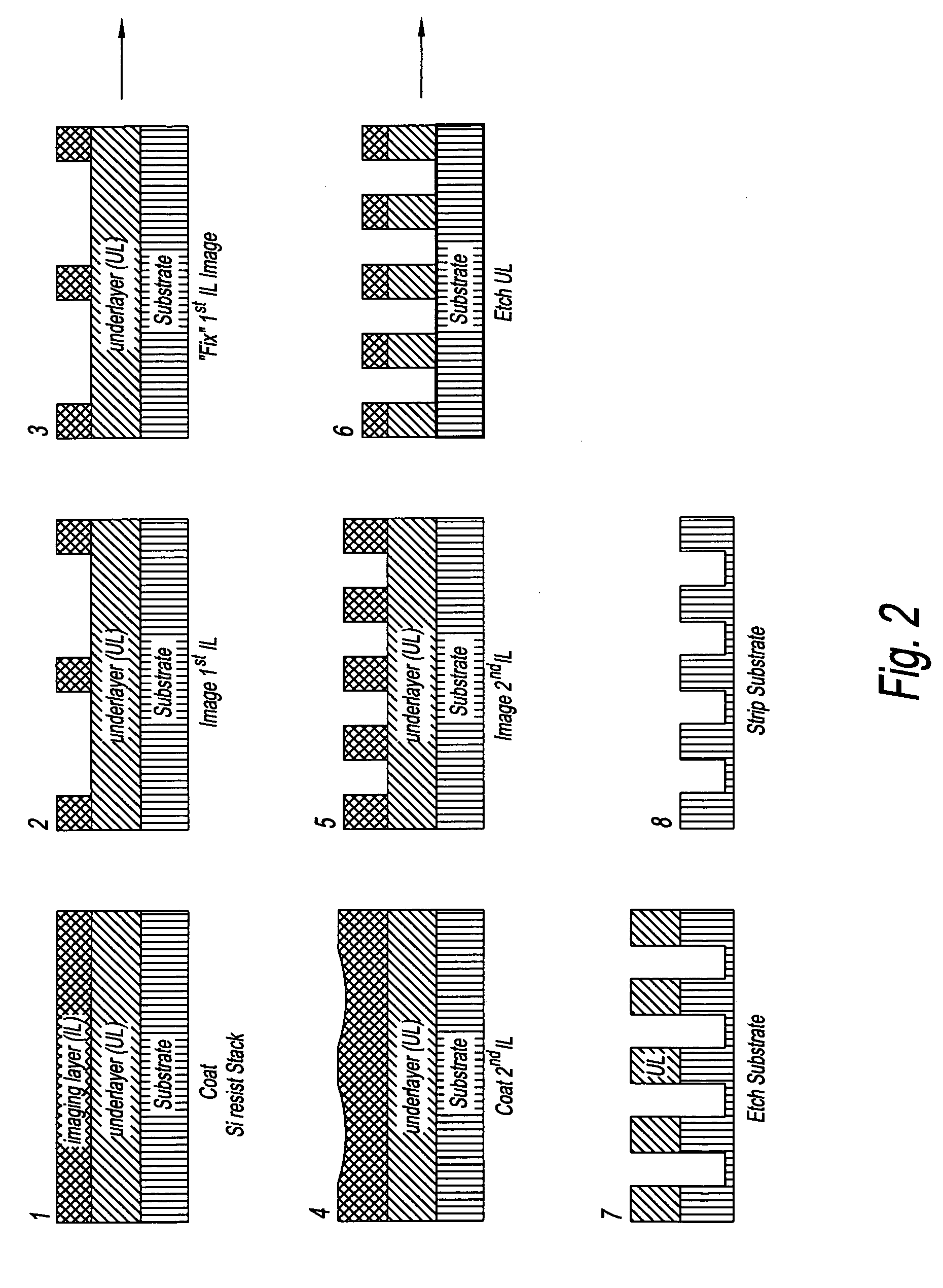
[0267]In this example, double patterning is demonstrated using a bottom anti-reflective coating (ARC) in combination with a non-silicon containing resist. The first image is patterned using General Lithographic Procedure 2 with the following exceptions. In the first exception, the UL is replaced with a BARC (ARC29A; supplied by Brewer Science, Inc.) and is coated to a 90 nm film thickness. In the second exception, a resist comprising a non-silicon containing polymer with incorporated anhydride functionality as described in U.S. Pat. No. 5,843,624, is used as a substitute for the imaging layer. The resulting image is fixed using the puddle process (PP) employing Fixer Formulation 62. The fixing procedure also uses a 30 second rinse-before-bake (RBB) process and a 175° C. post-fix bake temperature with duration of 90 seconds and. The resulting stack is then subjected to the General Lithographic Procedure 4 in which a resist comprising a non-silicon cont...


PUM


Abstract

Manufacturing semiconductor device by steps of:
    • a) providing substrate with antireflective coating or underlayer,
    • b) applying first photosensitive composition over substrate,
    • c) exposing first composition to radiation to produce first pattern,
    • d) developing exposed first composition to produce an imaged bilayer stack,
    • e) rinsing the stack,
    • f) applying fixer to the stack,
    • g) applying optional bake,
    • h) rinsing the stack,
    • i) applying second optional bake,
    • j) applying second photosensitive composition onto the stack to produce multilayer stack,
    • k) exposing second composition to produce second pattern offset from first pattern,
    • l) developing exposed second composition to produce multilayer stack, and
    • m) rinsing multilayer stack;
the photosensitive compositions have photoacid generator and substantially aqueous base insoluble polymer whose solubility increases upon treatment with acid and further comprises an anchor group, and the fixer is a polyfunctional compound reactive with anchor group, but does not contain silicon and the substrate stays within a lithographic cell from at least first coating step until at least after final exposure.

Description

RELATED APPLICATIONS[0001]This application claims priority of U.S. Provisional Patent Application No. 60 / 873,117, filed Dec. 6, 2006 and U.S. Provisional Patent Application No. 60 / 902,213, filed Feb. 20, 2007.FIELD OF THE INVENTION[0002]The present invention relates to a process of manufacturing a semiconductor device. More specifically, the present invention relates to a multiple exposure patterning process to manufacture relief images used in manufacture of a semiconductor device wherein the semiconductor substrate stays within a lithographic cell from the first coating step until at least after the final exposure.BACKGROUND TO THE INVENTION[0003]The trend in the IC industry is to print smaller and smaller critical dimensions (CD's). The critical dimensions within an integrated circuit are defined by a reticle or mask pattern, and an exposure tool which projects the image from the reticle onto a substrate. To achieve the trend toward size reduction for semiconductor devices, the i...

Claims


Application Information

Patent Timeline
IPC IPC(8): H01L21/00
CPCG03F7/095G03F7/0035G03F7/091G03F7/168G03F7/7045G03F7/70466H01L21/6715
Inventor BRZOZOWY, DAVESARUBBI, THOMAS R.MALIK, SANJAYSPAZIANO, GREGORY
Owner FUJIFILM ELECTRONICS MATERIALS US
Why Eureka
Try Eureka