Circuit substrate and method of manufacturing the same
a technology of circuit substrate and manufacturing method, which is applied in the direction of cable/conductor manufacturing, conductive pattern formation, insulation conductor/cable, etc., can solve the problems of large number of through holes, limited wiring layout, and difficulty in applying this method to fine through holes provided in semiconductor substrates having a reduced thickness, etc. cost reduction
- Summary
- Abstract
- Description
- Claims
- Application Information
AI Technical Summary
Benefits of technology
Problems solved by technology
Method used
Image
Examples
first embodiment
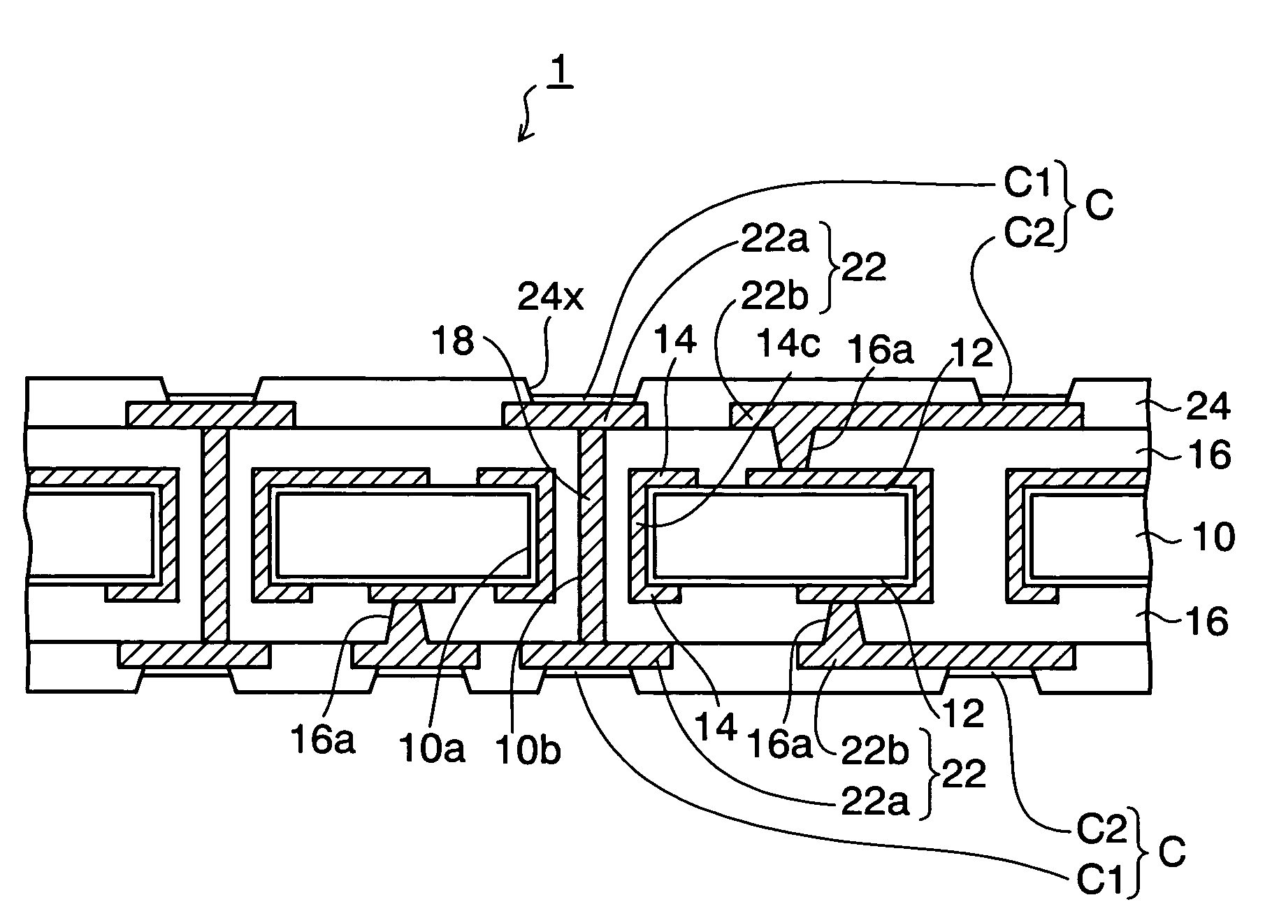
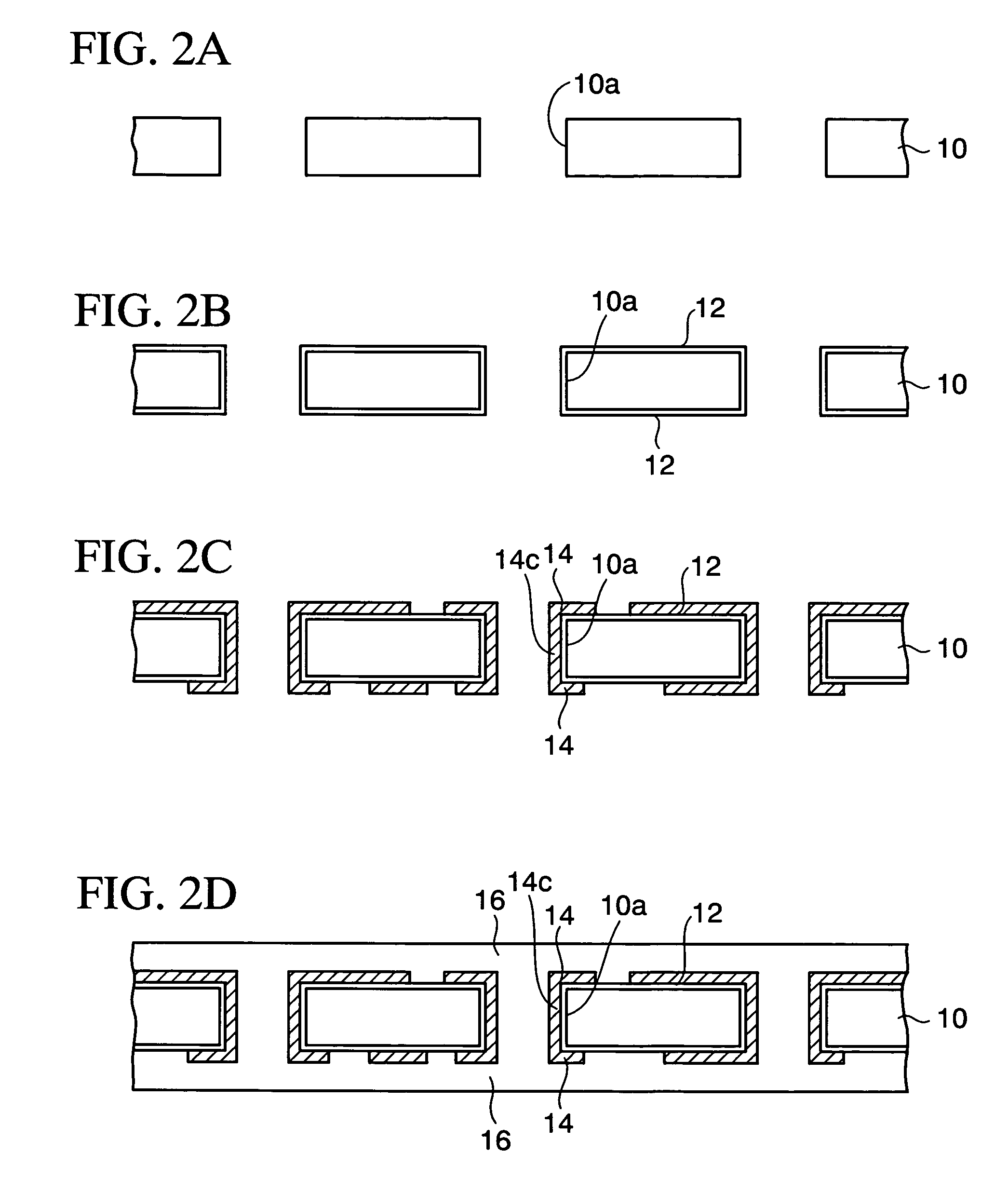
[0028]FIGS. 2A to 2I are cross-sectional views showing a method of manufacturing a circuit substrate of a first embodiment of the present invention. FIG. 3 is a cross-sectional view showing the circuit substrate of the first embodiment. FIGS. 4A to 4D are cross-sectional views showing details of the step of FIG. 2C. FIGS. 5A to 5C are cross-sectional views showing details of the step of FIG. 2F.
[0029]First, as shown in FIG. 2A, a silicon substrate 10 is prepared as a semiconductor substrate, and first through holes 10a are formed which penetrate the silicon substrate 10 in the thickness direction thereof. As a method of forming the first through holes 10a, a method is employed in which a mask (not shown) having opening portions provided therein is formed on the silicon substrate 10 and in which the silicon substrate 10 is etched by RIE through the opening portions of the mask. In this embodiment, since the silicon substrate 10 thickness of which is reduced to 50 to 300 μm (preferabl...
second embodiment
[0049]FIGS. 6A to 6G are cross-sectional views showing a method of manufacturing a circuit substrate of a second embodiment of the present invention.
[0050]The second embodiment differs from the first embodiment in that the second insulating layer 16 which covers the outer through conducting portions 14c on the inner surfaces of the first through holes 10a is formed by CVD. In the second embodiment, steps similar to those of the first embodiment will not be described in detail.
[0051]First, as shown in FIG. 6A, the same structure as in FIG. 2C is formed by a method similar to that of the first embodiment. That is, the first wiring layers 14 connected to each other via the outer through conducting portions 14c on the inner surfaces of the first through holes 10a are respectively formed on both sides of the silicon substrate 10. Then, as shown in FIG. 6B, the second insulating layer 16 is formed on the first wiring layers 14 on both sides of the silicon substrate 10 and the outer throug...
PUM
| Property | Measurement | Unit |
|---|---|---|
| thickness | aaaaa | aaaaa |
| diameter | aaaaa | aaaaa |
| diameter | aaaaa | aaaaa |
Abstract
Description
Claims
Application Information
 - R&D
- Intellectual Property
- Life Sciences
- Materials
- Tech Scout
- Unparalleled Data Quality
- Higher Quality Content
- 60% Fewer Hallucinations
Browse by: Latest US Patents, China's latest patents, Technical Efficacy Thesaurus, Application Domain, Technology Topic, Popular Technical Reports.
© 2025 PatSnap. All rights reserved.Legal|Privacy policy|Modern Slavery Act Transparency Statement|Sitemap|About US| Contact US: help@patsnap.com


