Circuit component module, electronic circuit device, and method for manufacturing the circuit component module

a technology of electronic circuit and component module, which is applied in the direction of conductive pattern formation, semiconductor/solid-state device details, electrical apparatus contruction details, etc., can solve the problems of reducing the number and affecting the quality of components. , to achieve the effect of reducing the number of parts, enhancing the thermal conductivity, and reducing the number of heat-releasing plates for each electronic componen

Inactive Publication Date: 2009-04-07
ALPS ALPINE CO LTD
View PDF12 Cites 34 Cited by
  • Summary
  • Abstract
  • Description
  • Claims
  • Application Information

AI Technical Summary

Benefits of technology

[0008]In view of the above disadvantages, the present invention provides a circuit component module that can be produced with high precision and reliability at low cost and a method for manufacturing the same. The present invention also provides an electronic circuit device from which heat generated from an electronic component generating a large amount of heat, such as a power IC, can be efficiently removed.

Problems solved by technology

This module therefore might not be able to maintain good precision in joining components disadvantageously because of uneven resin surfaces.
In addition, resin residues on the chip pad are likely to cause continuity failures, or stress produced between a component and the resin is liable to give damage to their junction.
In the circuit component module disclosed in Japanese Unexamined Patent Application Publication No. 11-220262 as well, heat or stress applied in the manufacturing process is liable to give damage to junctions.
Also, this process requires many steps for pattern alignment, consequently reducing the finished precision and increasing manufacturing cost.

Method used


Image

  • Circuit component module, electronic circuit device, and method for manufacturing the circuit component module
  • Circuit component module, electronic circuit device, and method for manufacturing the circuit component module
  • Circuit component module, electronic circuit device, and method for manufacturing the circuit component module

Examples


first embodiment

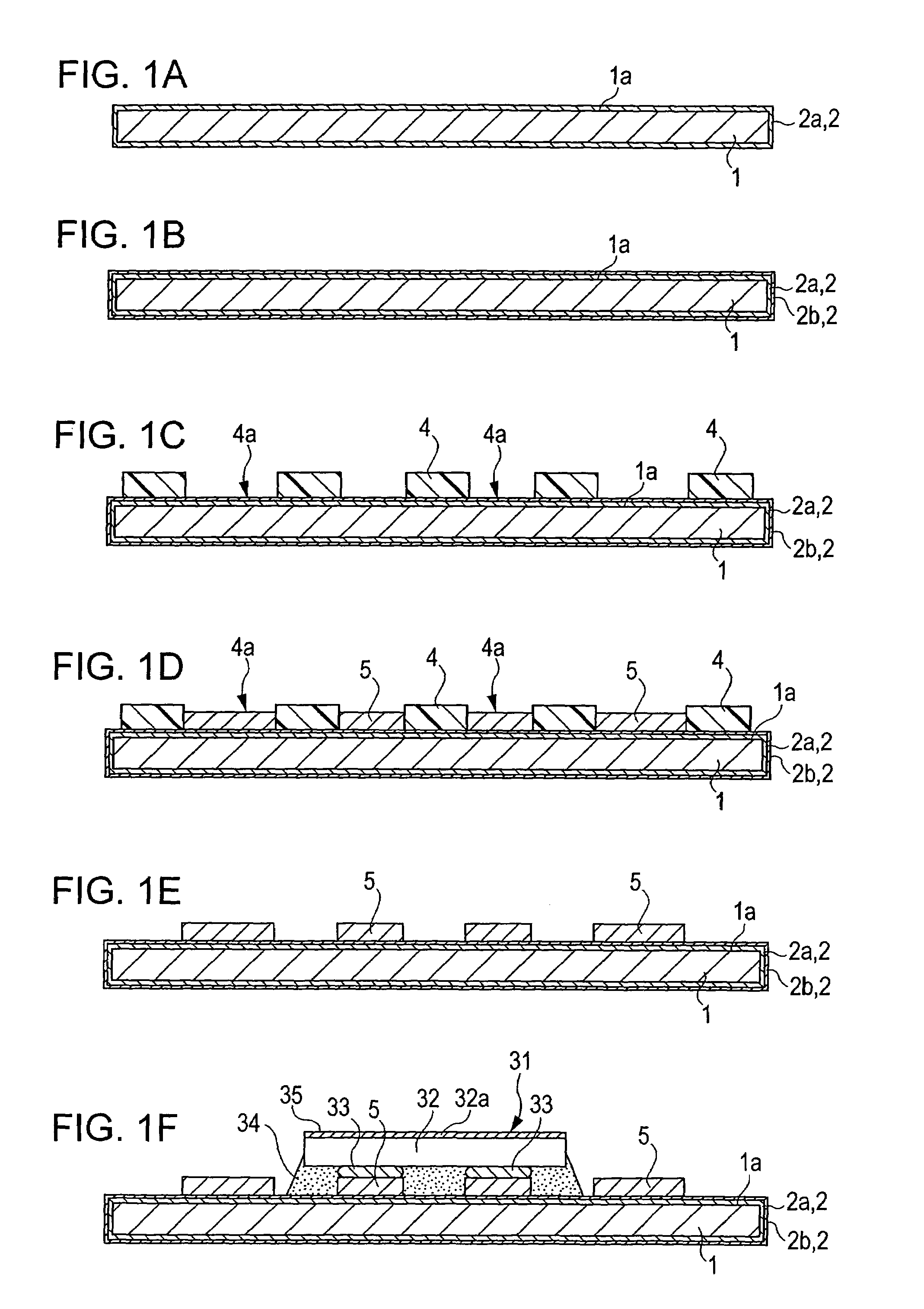
[0041]A circuit component module according to a first embodiment of the present invention and a method for manufacturing the same will now be described with reference to the drawings.

[0042]In the present embodiment, the method for manufacturing a circuit component module includes the mounting step of forming a seed layer and a wiring pattern on a base plate and mounting an electronic component on the base plate; the stacking step of stacking a first resin film and a heat-releasing plate on the base plate; and the removal step of removing the base plate and the seed layer.

[0043]In the mounting step, a seed layer is deposited on a base plate, and a wiring pattern is formed on the seed layer. Subsequently, an electronic component is mounted on the wiring pattern. In the stacking step, a first resin film having a pass-through hole and a heat-releasing plate are stacked on the base plate so that the electronic component is housed in the pass-through hole. In the removal step, the base pl...

second embodiment

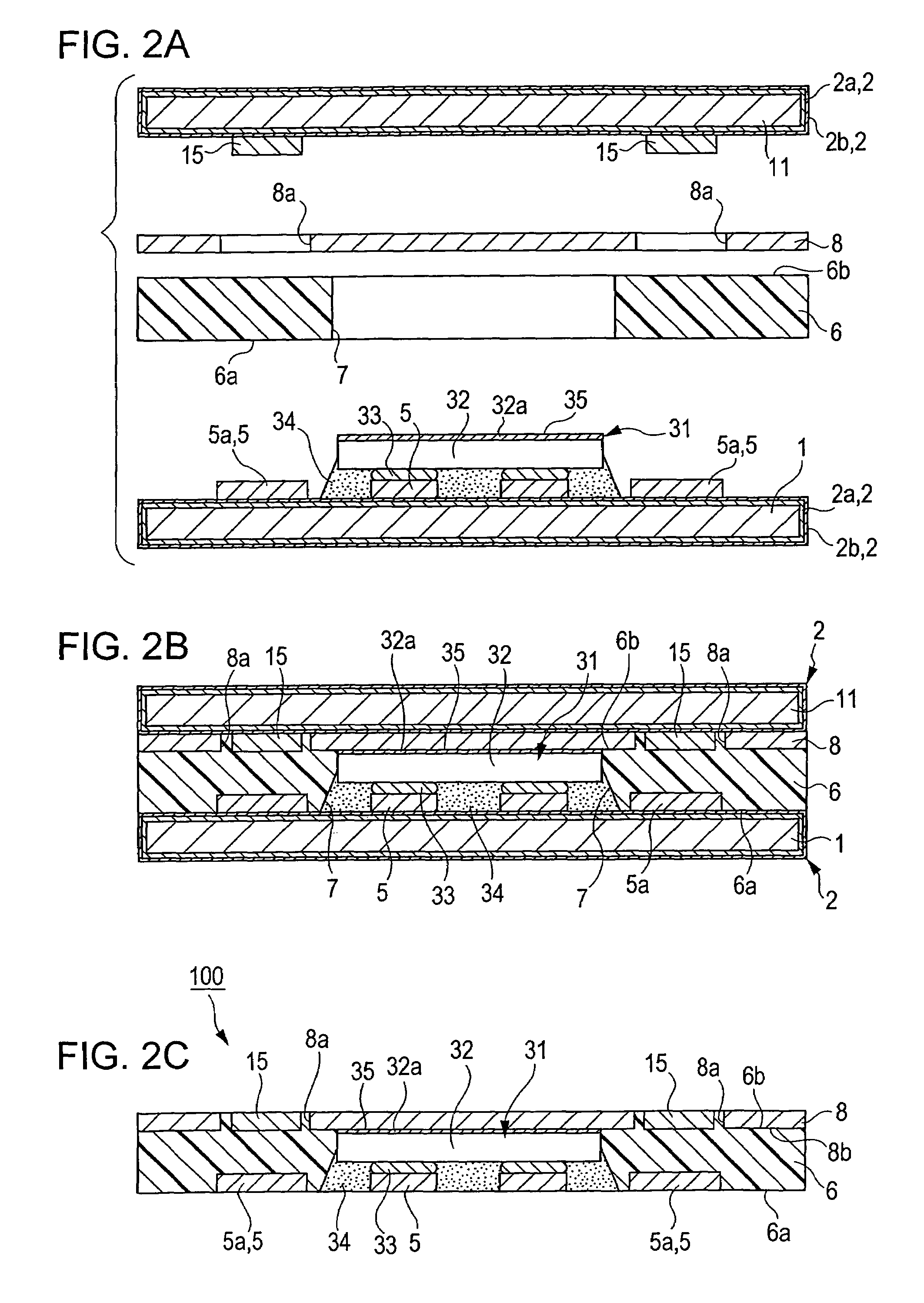
[0082]A circuit component module unit and its manufacturing method according to a second embodiment of the present invention will now be described. FIGS. 4A to 4C show a stacking step and a removal step of the method. The drawings referred to in the present embodiment are intended to illustrate the circuit component module and its manufacturing method, but do not necessarily correctly show its dimensional proportions according to the dimensions of the circuit component module unit used in practice.

Method for Manufacturing a Circuit Component Module Unit:

[0083]First, two base plates 1, two first resin films 6, and heat-releasing plate 8 are prepared as shown in FIG. 4A.

[0084]The base plate 1, which is the same as in the first embodiment, is coated with the seed layer 2 and has a wiring pattern 5 and the power IC 31. The first resin film 6 is a thermoplastic resin or glass epoxy plate with a thickness of about 100 to 500 μm, and has a pass-through hole 7. The heat-releasing plate 8 is...

third embodiment

[0099]FIG. 6 is a schematic sectional view of an electronic circuit device 500 according to a third embodiment. This electronic circuit device 500 includes the circuit component modules 100 of the first embodiment, and the first resin films 6 of the circuit component modules 100 are opposed to each other with the second resin film 106 therebetween. These resin films are bonded together to be integrated. Each circuit component module 100 has a heat-releasing plate 508 with a thickness of about 20 to 500 μm, doubling as an armoring plate. The heat-releasing plate 508 is bonded to the heat-releasing portion 32a of the power IC 31 with a thermally conductive adhesive 35.

[0100]The electronic circuit device 500 has the heat-releasing plates 508 doubling as the armoring plates that block external radio waves for signals transmitted through the wiring pattern 5 or a radiated electromagnetic field of the signals. In the electronic circuit device 500, the heat-releasing plates 508, the first ...


PUM

PropertyMeasurementUnit
thicknessaaaaaaaaaa
thicknessaaaaaaaaaa
thicknessaaaaaaaaaa

Abstract

A circuit component module includes a heat-releasing plate, a resin film stacked on a surface of the heat-releasing plate, an electronic component embedded in the first resin film and partially in contact with the heat-releasing plate, and a wiring pattern embedded in the surface of the first resin film opposite the heat-releasing plate. The wiring pattern forms a circuit in combination with the electronic component.

Description

BACKGROUND OF THE INVENTION[0001]1. Field of the Invention[0002]The present invention relates to a circuit component module and an electronic circuit device, and to a method for manufacturing the circuit component module.[0003]2. Description of the Related Art[0004]Portable electronic devices, such as cellular phones and PDAs, are increasingly using sheet-like circuit component modules in which a circuit board and various components are integrated in order to reduce the size and weight and the cost. Such a circuit component module includes various components embedded in, for example, a resin base plate and an electroconductive circuit pattern formed on the surface, and is formed on an almost even flat plate, as disclosed in, for example, Japanese Unexamined Patent Application Publication Nos. 2001-358465 and 11-220262. Since the circuit component module thus can be small and lightweight and excels at mass production, it is suitable as a component circuit used in portable electronic ...

Claims


Application Information

Patent Timeline
Patent Type & Authority Patents(United States)
IPC IPC(8): H05K1/00
CPCH01L23/3107H01L23/36H01L23/4334H01L25/0657H01L25/105H05K1/187H01L21/568H01L21/563Y10T29/49128H01L21/6835H01L23/49575H01L2224/16H01L2224/73203H01L2224/73253H01L2225/06524H01L2225/06541H01L2225/06555H01L2225/06586H01L2225/06589H01L2924/01078H01L2924/01079H01L2924/3025H05K1/0203H05K1/0207H05K3/205H05K3/4614H05K3/4641H05K2201/10515H05K2201/10674H05K2203/063H01L2224/73204H01L2225/1035H01L2225/1058Y10T29/49155H01L2924/00014H01L2924/00011H01L2224/0401
Inventor SASAKI, YORIHIKO
Owner ALPS ALPINE CO LTD
Why Eureka
Try Eureka