Display device with light emitting elements

a technology of light-emitting elements and display devices, which is applied in the direction of static indicating devices, solid-state devices, instruments, etc., can solve the problems of deteriorating manufacturing yield, difficult to control uniformly the illumination intensity of lasers within the plane of glass substrates, and difficult to produce display currents. accurate and reproducible

Active Publication Date: 2007-05-22
RAKUTEN GRP INC
View PDF17 Cites 22 Cited by
  • Summary
  • Abstract
  • Description
  • Claims
  • Application Information

AI Technical Summary

Benefits of technology

[0038]An object of the invention is to provide a display device provided with a light-emitting element of a current drive type, and particularly a structure of the display device, which accurately produces a display current for gray-scale expression without imposing an excessively load on a manufacturing process.
[0042]Accordingly, the invention has the following major advantage. The current for executing the gray-scale expression based on the display signal of the weighted n bits (n: integer larger than two) is formed of a sum of the output currents of the one analog current supply circuit for representing the lower k bits (k: integer satisfying (2≦k≦(n−1))) and the j digital current supply circuits corresponding to the higher j bits (j: integer equal to (n−k)). Thereby, the current for the whole gray-scale range can be provided by the current supply circuits smaller in number than the bits of the display signal. Accordingly, a circuit area or footprint can be smaller than that of a structure, in which digital current supply circuits of n in number provide the current for the whole gray-scale range. Further, variations in current, which may occur in a high gray level region, i.e., in a large current region due to variations in element characteristics, can be reduced as compared with the case, in which a single analog current supply circuit generates the current for the whole gray-scale range.
[0043]The current for executing the gray-scale expression based on the display signal of the weighted n bits (n: integer larger than two) is formed of the sum of the output currents of the analog current supply circuit for representing the lower k bits (k: integer satisfying (2≦k≦(n−1))) and the analog current supply circuit for representing the higher j bits (j: integer equal to (n−k)). Thereby, the current for the whole gray-scale range can be provided by the current supply circuits smaller in number than the bits of the display signal. Accordingly, the circuit footprint can be smaller than that of the structure, in which digital current supply circuits of n in number provide the current for the whole gray-scale range. Further, variations in current, which may occur in a high gray level region, i.e., in a large current region due to variations in element characteristics, can be reduced as compared with the case, in which a single analog current supply circuit generates the current for the whole gray-scale range.
[0044]The current, which are used for the 2n gray levels, and more specifically for executing the gray-scale expression based on the display signal of weighted n bits (n: integer larger than two), is generated in a sharing manner by plurality of analog current supply circuits, which are provided corresponding to the plurality of current ranges, respectively, and each have the function of performing the calibration at predetermined point in the corresponding current range. Therefore, the current for the whole gray-scale range can be provided by the current supply circuits smaller in number than the bits of the display signal. Accordingly, the circuit footprint can be smaller than that of the structure, in which only the digital current supply circuits of n in number provide the current for the whole gray-scale range. Further, variations in current, which may occur in a high gray level region, i.e., in a large current region due to variations in element characteristics, can be reduced as compared with the case, in which a single analog current supply circuit generates the current for the whole gray-scale range.

Problems solved by technology

This results in severe requirement relating to the manufacturing variations, and thus deteriorates the manufacturing yield.
Consequently, if the number of gray levels is large, it is impossible to ignore the influence by the variations in output current within a region of high gray level (large output current), and gray-scale shift may occur.
However, the low-temperature polycrystalline silicon TFT is generally formed by laser anneal, and it is difficult to control uniformly a laser illumination intensity within a plane of a glass substrate.
Accordingly, the display device using the low-temperature polycrystalline silicon TFTs cannot reliably have an intended data current accuracy for gray-scale expression without difficulty.

Method used


Image

  • Display device with light emitting elements
  • Display device with light emitting elements
  • Display device with light emitting elements

Examples


first embodiment

[0071

[0072](Whole Structure of Display Device)

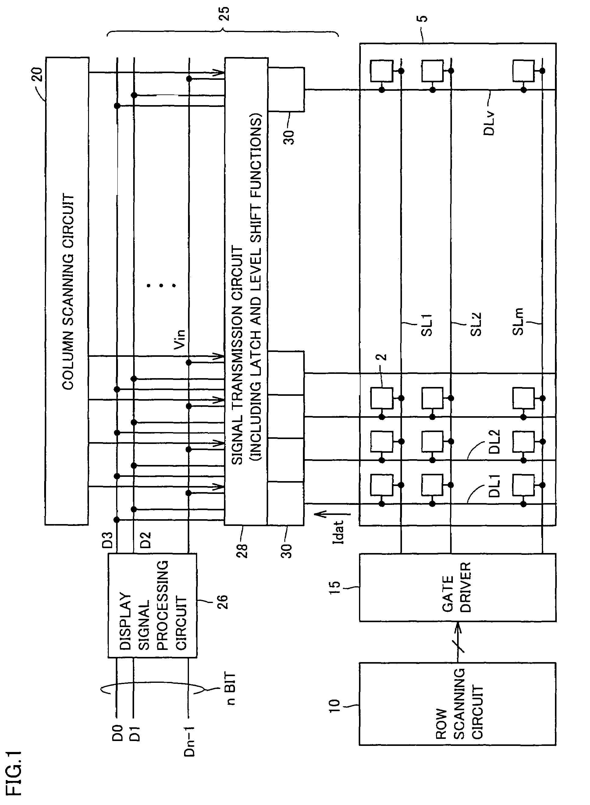
[0073]Referring to FIG. 1, a display device 1 according to the invention includes a display panel portion 5, in which a plurality of pixels 2 are arranged in rows and columns, a row scanning circuit 10, a gate driver 15, a column scanning circuit 20 and a source driver 25.

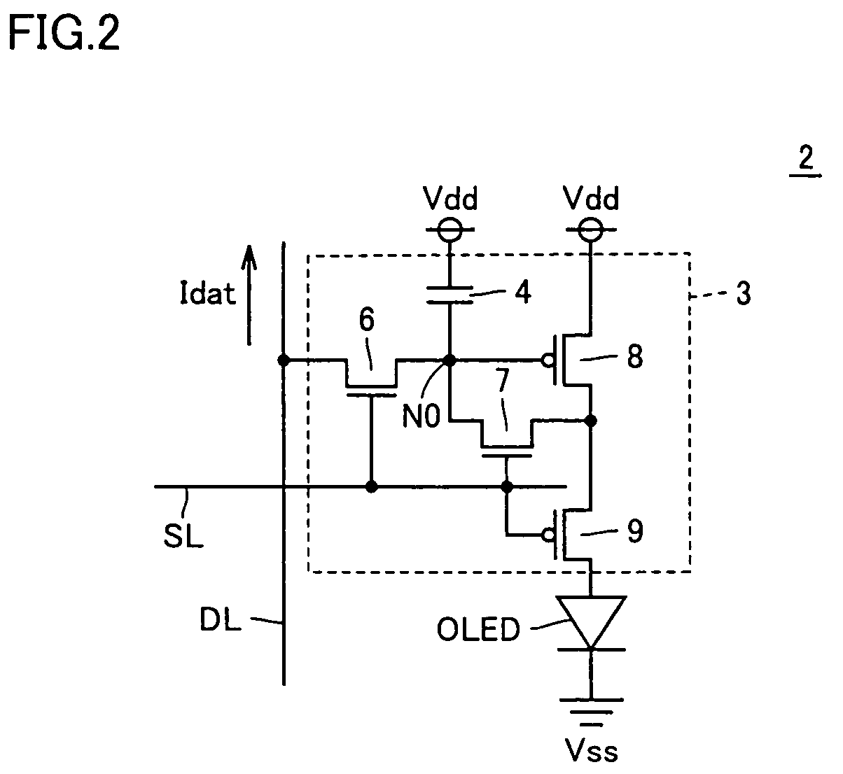
[0074]Each pixel 2 has a light-emitting element of a current drive type such as an EL element or LED, as will be described later. In display panel portion 5 having the plurality of pixels 2 arranged in rows and columns, scanning lines SL1, SL2–SLm (m: natural number) are arranged corresponding to the rows of pixels (which may be simply referred to as “pixel rows” hereinafter), respectively, and data lines DL1, DL2–DLv (v: natural number) corresponding to the columns of pixels (which may be simply referred to as “pixel columns” hereinafter), respectively.

[0075]Row scanning circuit 10 successively selects the pixel rows at predetermined scanning cycles. Gate driver 15 suc...

second embodiment

[0129

[0130]Description will now be given on embodiments relating to several forms of the structure of data current generating circuit 30 shown in FIG. 1. In the embodiments described below, data current generating circuit 30 in the display device of the invention shown in FIG. 1 is replaced with data current generating circuits of second and further embodiments, respectively.

[0131]Referring to FIG. 6, a data current generating circuit 31 according to a second embodiment differs from data current generating circuit 30 of the first embodiment in that analog current supply circuit 400 is replaced with an analog current supply circuit 100.

[0132]Similarly to data current supply circuit 30, digital current supply circuits 70 are provided corresponding to data bits D2 and D3, respectively, and operate to execute or stop the production of bit-weighted currents, i.e., currents I4 and I8 in response to the levels of data bits D2 and D3, respectively.

[0133]Analog current supply circuit 100 sel...

third embodiment

[0151

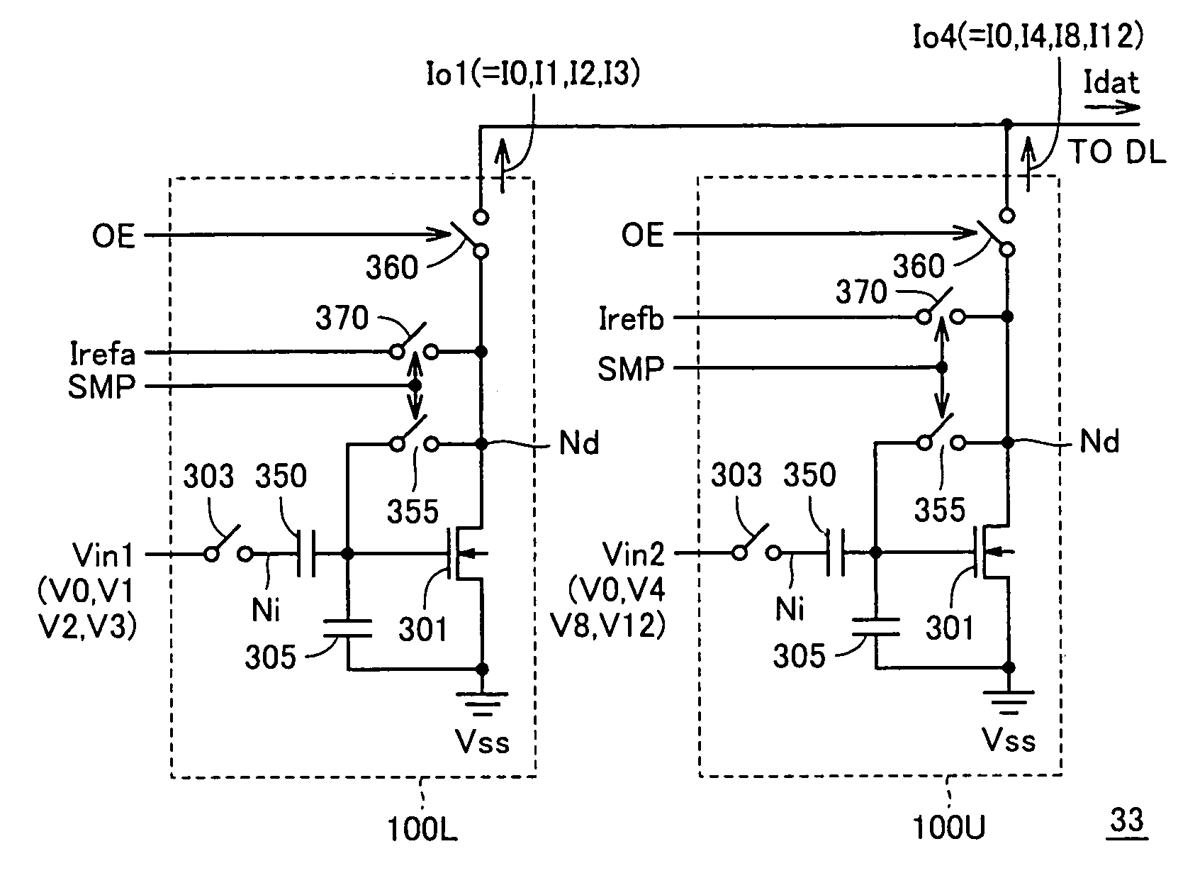
[0152]Referring to FIG. 9, a data current generating circuit 32 according to a third embodiment includes one analog current supply circuit 100 and one analog current supply circuit 400. The structures of analog current supply circuits 100 and 400 are the same as those already described, and therefore description thereof is not repeated.

[0153]Analog current supply circuit 400 is supplied with input voltage Vin1 having one of levels of voltages V0–V3 corresponding to currents I0–I3, respectively. Analog current supply circuit 100 is supplied with input voltage Vin2 set to one of voltages V0, V4, V8 and V12 corresponding to currents I0, I4, I8 and I12, respectively.

[0154]Input voltage Vin1 is produced in accordance with lower data bits D0 and D1 by display signal processing circuit 26 shown in FIG. 1, similarly to input voltage Vin in the first and second embodiments. Input voltage Vin2 is produced in accordance with higher data bits D2 and D3 by display signal processing circuit ...


PUM


Abstract

A display current of a whole gray scale range according to a display signal of four bits is produced from a sum of output currents of an analog current supply circuit producing a first output current according to lower data bits and two digital current supply circuits operating in accordance with corresponding data bits to execute or stop generation of second and third output currents according to higher data bits. The analog current supply circuit has a calibration function of compensating for output current variations due to transistor characteristics at one point in a control range of the first output current. A display device with light-emitting elements can accurately generate a display current for gray-scale expression without imposing an excessive load on a manufacturing process while suppressing circuit footprint.

Description

BACKGROUND OF THE INVENTION[0001]1. Field of the Invention[0002]The present invention relates to a display device, and particularly to a display device including a light-emitting element, such as an organic EL (Electro Luminescence), which varies its light-emitting luminance according to a drive current, in each of pixels and executing gray-scale expression based on a digital signal.[0003]2. Description of the Background Art[0004]As a display device of a flat-panel type, attention has been given to a display device of a self-light-emitting type, in which each pixel is formed of a light-emitting element of a current drive type. The display device of the self-light-emitting type has high visibility as well as high moving picture quality. A light-emitting diode (LED) is well known as a kind of light-emitting element of the current drive type.[0005]Generally, a display device includes a plurality of pixels, which are arranged in rows and columns, and are successively driven by dot-seque...

Claims


Application Information

Patent Timeline
Patent Type & Authority Patents(United States)
IPC IPC(8): G09G3/36G09G3/20H01L51/50G09G3/30G09G3/32
CPCG09G3/325G09G3/3283G09G2300/0842G09G2310/0254G09G2310/027G09G2320/043G09G2330/028
Inventor HASHIDO, RYUICHITOKIOKA, HIDETADAAGARI, MASAFUMIGOTO, SUEHIROURAKABE, TAKAHIRO
Owner RAKUTEN GRP INC
Why Eureka
Try Eureka