Flat display panel and assembly process or driver components in flat display panel

a technology of flat display panel and assembly process, which is applied in the direction of printed circuits, instruments, optics, etc., can solve the problems that none of these techniques are economically desirable, and achieve the effect of reducing material cost and processing tim

Active Publication Date: 2009-04-07
AU OPTRONICS CORP
View PDF9 Cites 27 Cited by
  • Summary
  • Abstract
  • Description
  • Claims
  • Application Information

AI Technical Summary

Benefits of technology

[0011]The present invention provides an electrical connection structure and an assembly process that can reduce the material cost and processing time in the assembly of driver components in a flat display panel.

Problems solved by technology

None of these techniques is economically desirable.

Method used


Image

  • Flat display panel and assembly process or driver components in flat display panel
  • Flat display panel and assembly process or driver components in flat display panel
  • Flat display panel and assembly process or driver components in flat display panel

Examples


Embodiment Construction

)

[0021]The present invention describes an electrical connection structure and an assembly process that can reduce the material cost and processing time in the assembly of driver components in a flat display panel. In exemplary implementations, the following description depicts embodiments in which the flat display panel is a LCD panel. However, the structure and assembly process of the invention are intended to be generally suitable with any types of displays such as electroluminescent displays, plasma displays or the like.

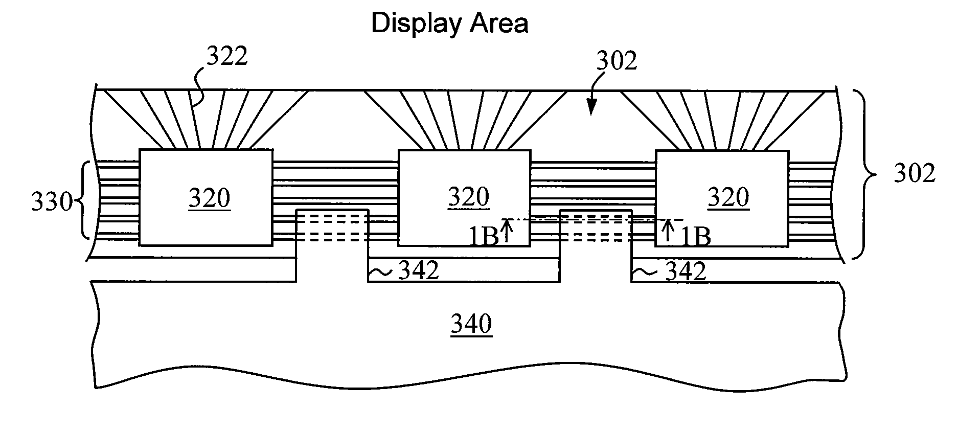
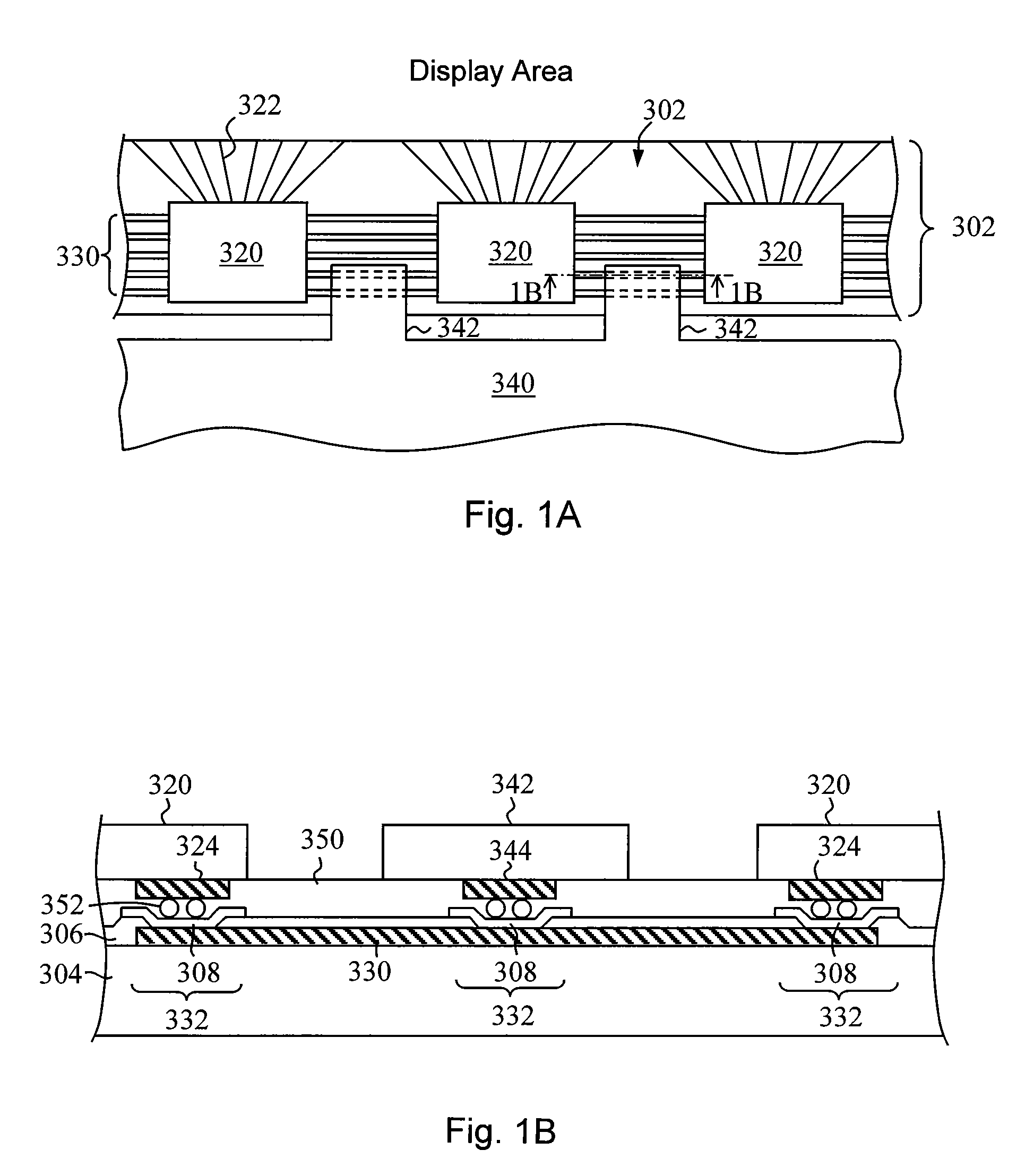
[0022]FIG. 1A is a schematic view illustrating the connection scheme of driver components in a LCD panel according to an embodiment of the invention. In a peripheral non-display area 302 of the LCD panel are a plurality of driver ICs 320. The driver ICs 320 couple via wiring lines 322 to pixel elements (not shown) located in the display area. The driver ICs 320 can be scan driver ICs or data driver ICs configured to deliver either addressing or image data signals ...


PUM

PropertyMeasurementUnit
temperatureaaaaaaaaaa
conductiveaaaaaaaaaa
anisotropic conductiveaaaaaaaaaa

Abstract

A flat display panel comprises a plurality of driver ICs and one or more flexible printed circuit, a plurality of common wires formed on the substrate to electrically connect the ICs to the one or more flexible printed circuit, and at least one anisotropic conductive film that connects respective connecting terminals of the driver ICs and flexible printed circuit to terminals pads of the common wires. The anisotropic conductive film is laminated over the substrate to cover the terminal pads. The driver ICs and flexible printed circuit are aligned and attached on the anisotropic conductive layer by thermocompression bonding.

Description

BACKGROUND OF THE INVENTION[0001]1. Field of the Invention[0002]This invention generally relates to the field of flat display panel manufacture, and more particularly to the interconnection structure and the assembly process of driver components in flat display panels such as liquid crystal display (LCD) panels.[0003]2. Description of the Related Art[0004]The construction of flat display panels such as LCDs generally includes pixel cells arranged in array and driven by means of driver components placed at the peripheral area of the display area. The driver components are conventionally operable to output addressing and data image signals to the pixel cells to control the illumination or extinction for achieving image displaying.[0005]The driver components conventionally include scan driver integrated circuits (ICs) and data driver ICs along two peripheral sides of the display panel. Flexible printed circuits are coupled with the scan and data driver ICs to provide signals such as po...

Claims


Application Information

Patent Timeline
Patent Type & Authority Patents(United States)
IPC IPC(8): G02F1/1345G02F1/13G02F1/133G09G3/36H05K3/32H05K3/36
CPCG02F1/13452H05K3/323H05K3/361H05K2201/10674
Inventor LU, CHAO-LIANGYANG, CHIH-HSIANGLEE, KUO-CHIH
Owner AU OPTRONICS CORP
Why Eureka
Try Eureka