System and method for increased stand-off height in stud bumping process

a technology of flip chip and stand-off height, which is applied in the direction of auxillary welding devices, soldering apparatus, and semiconductor/solid-state device details, etc. it can solve the problems of increasing the size of the die, and reducing the clearance between the chip and the substrate, so as to increase the space, increase the stand-off height, and improve the effect of reliability

Active Publication Date: 2009-04-21
TEXAS INSTR INC
View PDF5 Cites 68 Cited by
  • Summary
  • Abstract
  • Description
  • Claims
  • Application Information

AI Technical Summary

Benefits of technology

[0013]An advantage of the present invention is the ability to manufacture stud bumps with increased stand-off heights in a single process rather than having to stack individual stud bumps on top of each other.
[0014]A further advantage of the present invention is an increase in the space between the chip and the substrate, which allows the underfill adhesive to flow more freely and to fill all the voids between the chip and the substrate. The present invention does not require the removal of the PBO or PIQ protective overcoat to create additional space between the chip and the substrate.
[0015]An additional advantage of the invention is that stronger, more reliable joints are produced using the larger stud bumps without the need for using excess amounts of solder to form the joints. The present invention can be used in both gold and copper stud bumping processes.
[0016]A further advantage of the present invention is the use of a tapered section at the tip of the capillary to ensure that adjacent stud bumps are not damaged during the formation of new stud bumps. The size of the tapered section may be selected to facilitate the production of stud bumps in ultra fine pitch bonding.

Problems solved by technology

When wire bond connections are used, they are limited to the perimeter of the die, which increases the die size as the number of connections increases.
The wire may be separated, for example, using a wire clamp to grab the gold wire while the wire and capillary are moved away from the ball, which causes the wire to break.
A disadvantage of this method is a reduction in the clearance between the chip and the substrate, which makes it more difficult for the underfill to fill all the voids in the device.
A further disadvantage is that using higher bonding force causes more stress on the die, which may damage the chip or stud bumps.
Forming two or more stud bumps on top of each other, results in a taller bump that increases the gap between the chip and the substrate, thereby increasing the space in which the underfill flows.
A disadvantage of using stacked stud bumps is the increase in manufacturing time that is needed to form the additional bumps.
A further disadvantage of this method is that the stacked stud bumps tend to be weaker than single bumps and the die undergoes additional stress to form the extra bumps.
A disadvantage of this method is poor die reliability because protection of the die surface has been removed.
Accordingly, the removal of the protective overcoat layer is not desired.

Method used


Image

  • System and method for increased stand-off height in stud bumping process
  • System and method for increased stand-off height in stud bumping process
  • System and method for increased stand-off height in stud bumping process

Examples


Embodiment Construction

[0024]Currently preferred embodiments for making and using the present invention are discussed in detail below. It should be appreciated, however, that the present invention provides many applicable inventive concepts that can be embodied in a wide variety of specific contexts. The specific embodiments discussed herein are merely illustrative of specific ways to make and use the invention, and they are not intended to limit the scope of the invention.

[0025]The present invention will be described with respect to preferred embodiments in a specific context, namely a flip chip assembly with gold stud bumps. The invention may also be applied, however, to other flip chip assemblies using other materials, such as copper, to form the stud bumps.

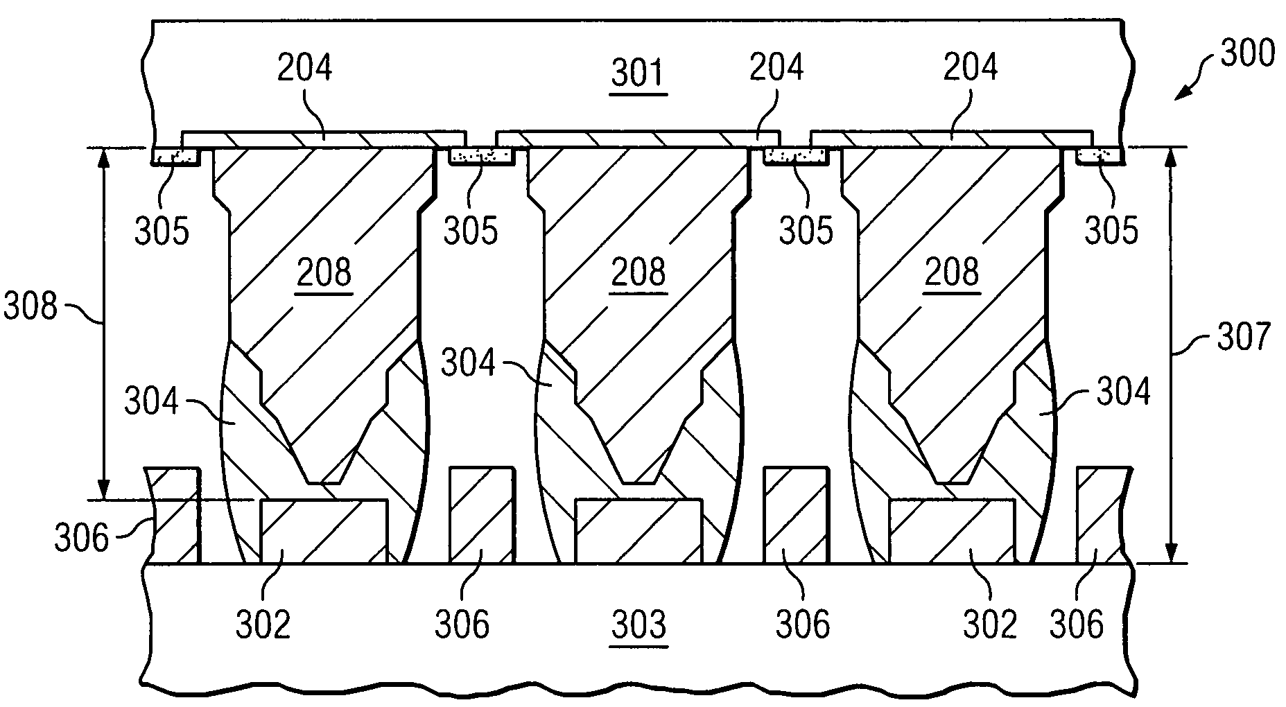
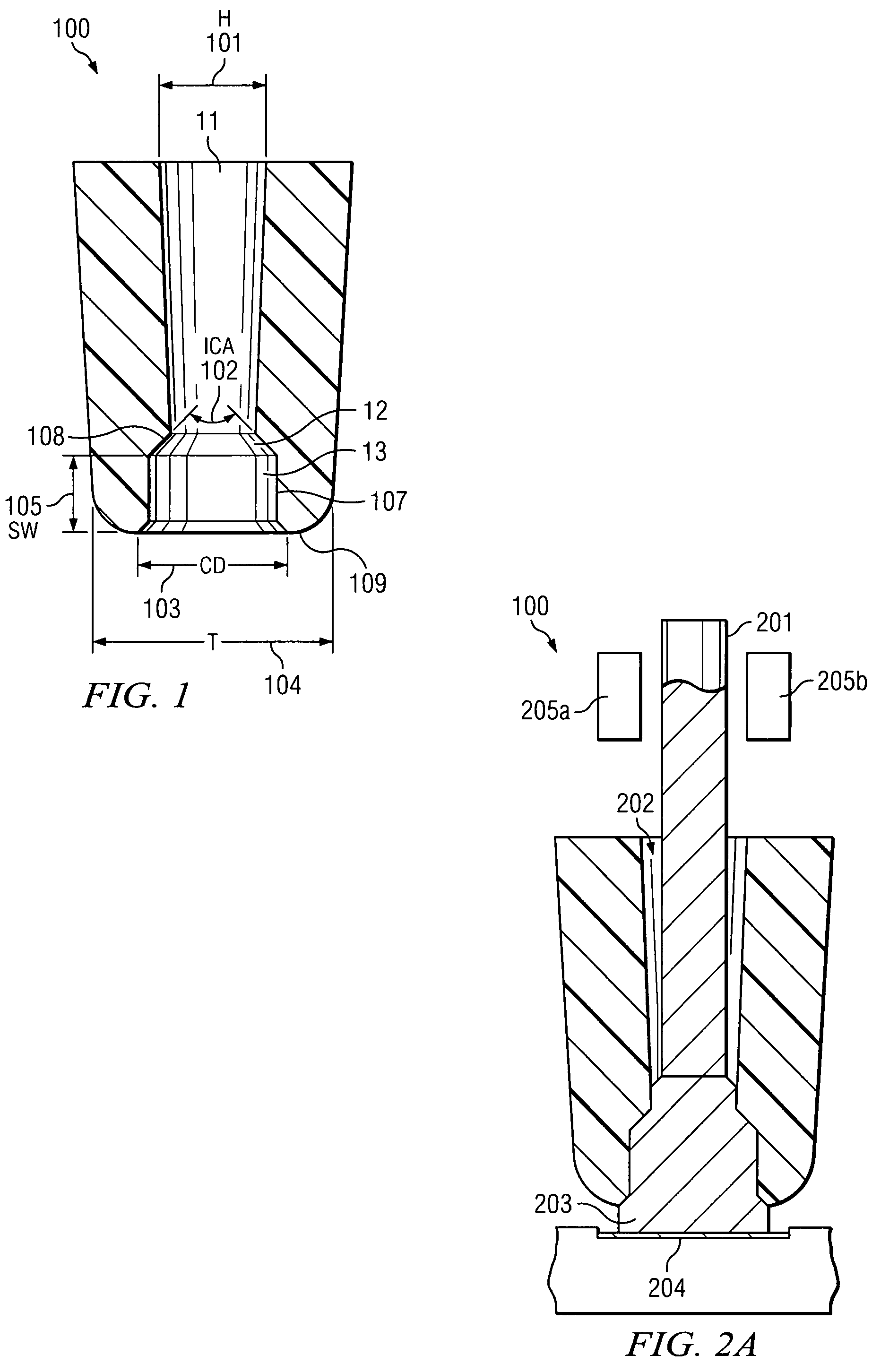
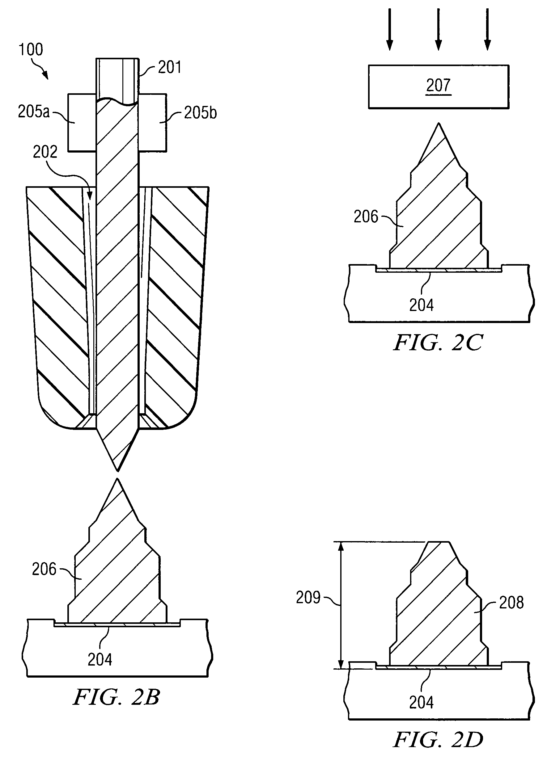
[0026]FIG. 1 is an exemplary embodiment of a novel capillary 100 that is designed to produce stud bumps with increased stand-off height. The dimensions of capillary 100 are hole diameter (H) 101, inside chamfer angle (ICA) 102, chamfer diameter (CD)...


PUM


Abstract

System and method for creating single stud bumps having an increased stand-off height. A preferred embodiment includes a method of using a capillary for creating stud bumps in a flip chip assembly, the capillary includes a hole section adapted to pass a wire, a chamfer section providing a transition from the hole section to a stud bump section, and a sidewall within the stud bump section, the sidewall having a sidewall height, wherein the side wall height is equal to, or greater than, the a diameter of the stud bump section.

Description

TECHNICAL FIELD[0001]The present invention relates generally to a system and method for manufacturing stud bumps in a flip chip assembly and, more particularly, to a system and method for manufacturing stud bumps with a higher stand-off height that results in stronger, more reliable joints.BACKGROUND[0002]In flip chip microelectronic assembly, electronic components or “chips” are connected face-down (i.e. “flipped”) onto substrates, circuit boards, or carriers by means of conductive bumps that are formed on the chip's bond pads. Flip chip assembly eliminates bond wires, greatly reduces induction and capacitance in connections, and shortens electrical paths, thereby providing a device with high speed electrical performance. When wire bond connections are used, they are limited to the perimeter of the die, which increases the die size as the number of connections increases. Flip chip connections use the whole area of the die, not just the perimeter, and can accommodate many more conne...

Claims


Application Information

Patent Timeline
Patent Type & Authority Patents(United States)
IPC IPC(8): H01L21/44H01L21/48H01L21/50
CPCH01L24/11H01L24/13H01L2224/1134H01L2224/13099H01L2224/13144H01L2224/78302H01L2924/01029H01L2924/01057H01L2924/01079H01L2924/30105H01L2924/01005H01L2924/01033H01L2924/014H01L2224/05567H01L2224/0557H01L2224/05573H01L2924/00014H01L2224/05571H01L2224/0554H01L2224/13017H01L2224/05599H01L2224/0555H01L2224/0556
Inventor MIRANDA, ARIEL LIZABACAMENFORTE, RAYMUNDO MONASTERIO
Owner TEXAS INSTR INC
Why Eureka
Try Eureka