Reproducible resistance variable insulating memory devices having a shaped bottom electrode

a resistance variable and memory device technology, applied in the field of random access memory (ram) devices, can solve the problems of not providing stable and reproducible switching, not providing memory properties in a controlled manner, etc., and achieve the effect of small curvature and enhanced local electric field

Active Publication Date: 2009-04-21
MICRON TECH INC
View PDF101 Cites 97 Cited by
  • Summary
  • Abstract
  • Description
  • Claims
  • Application Information

AI Technical Summary

Benefits of technology

[0007]The present invention relates to the use of a shaped bottom electrode in a resistance variable memory device. The shaped bottom electrode ensures that the thickness of the insulating material at the tip of the bottom electrode is thinnest, therefore creating the largest electric field at the tip of the bottom electrode. The small curvature of the electrode tip also enhances the local electric field. The arrangement of electrodes and the structure of the memory element makes it possible to create conduction paths with stable, consistent and reproducible switching and memory properties in the memory device.

Problems solved by technology

Unfortunately, the metal-insulator-metal (MIM) structure with a resistive film or insulting oxide sandwiched between two flat metallic electrode plates as disclosed in FIGS. 1 and 2 does not provide stable and reproducible switching and does not provide memory properties in a controlled manner, as the conduction path between the elements can occur anywhere in the resistive film or insulating oxide between the top and bottom electrodes.
The random and unpredictable conduction path between the elements is believed to be created by random and unpredictable defect sites in the deposited film.

Method used


Image

  • Reproducible resistance variable insulating memory devices having a shaped bottom electrode
  • Reproducible resistance variable insulating memory devices having a shaped bottom electrode
  • Reproducible resistance variable insulating memory devices having a shaped bottom electrode

Examples


Embodiment Construction

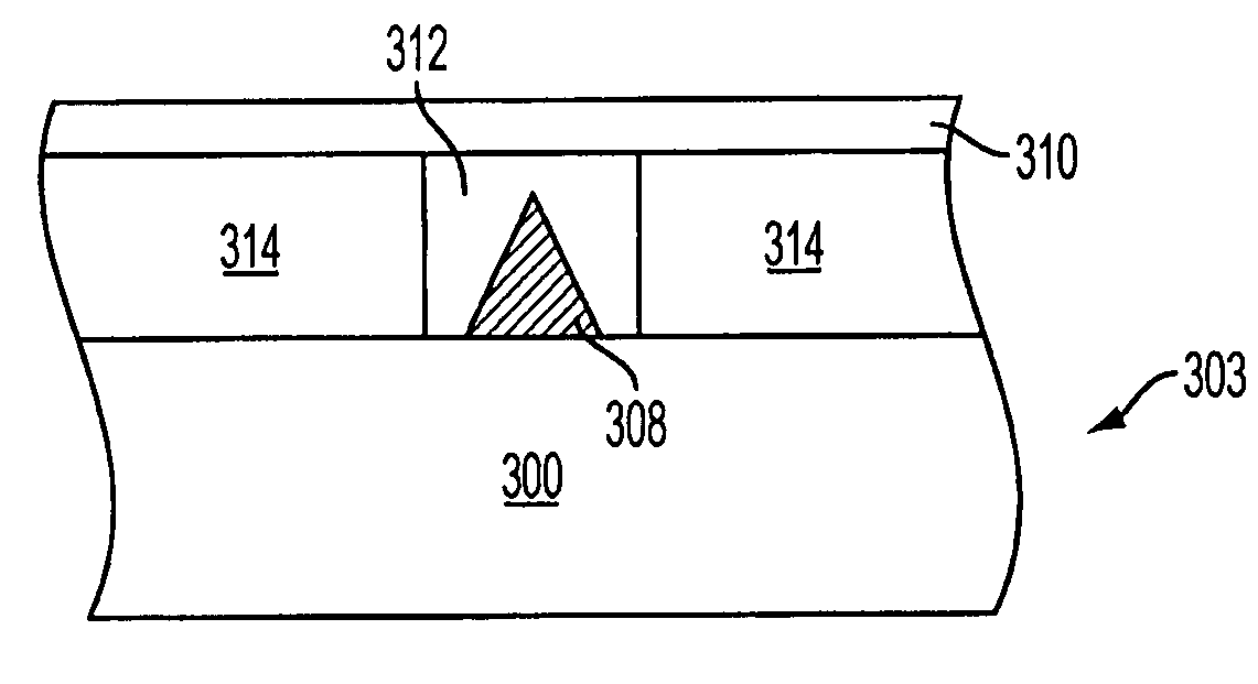
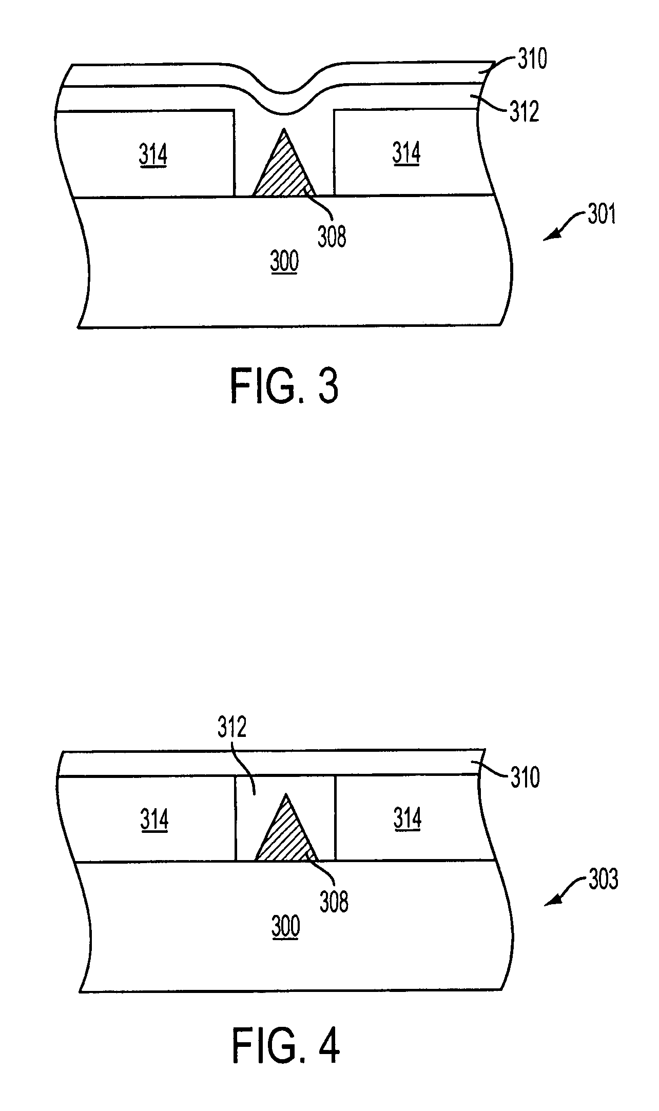
[0026]In the following detailed description, reference is made to the accompanying drawings, which form a part hereof and show by way of illustration specific embodiments in which the invention may be practiced. These embodiments are described in sufficient detail to enable those skilled in the art to practice the invention, and it is to be understood that other embodiments may be utilized, and that structural, logical, and electrical changes may be made without departing from the spirit and scope of the present invention. The progression of processing steps described is exemplary of embodiments of the invention; however, the sequence of steps is not limited to that set forth herein and may be changed as is known in the art, with the exception of steps necessarily occurring in a certain order.

[0027]The term “substrate” used in the following description may include any supporting structure including, but not limited to, a plastic, ceramic, semiconductor, or other substrate that has a...


PUM


Abstract

The present invention relates to the use of a shaped bottom electrode in a resistance variable memory device. The shaped bottom electrode ensures that the thickness of the insulating material at the tip of the bottom electrode is thinnest, creating the largest electric field at the tip of the bottom electrode. The arrangement of electrodes and the structure of the memory element makes it possible to create conduction paths with stable, consistent and reproducible switching and memory properties in the memory device.

Description

FIELD OF THE INVENTION[0001]The invention relates to the field of random access memory (RAM) devices formed using a resistance variable material, and in particular to an improved structure for, and a method of manufacturing, a resistance variable memory element.BACKGROUND OF THE INVENTION[0002]Resistance variable memory is a RAM that has electrical resistance characteristics that can be changed by external influences. The basic component of a resistance variable memory cell is a variable resistor. The variable resistor can be programmed to have high resistance or low resistance (in two-state memory circuits), or any intermediate resistance value (in multi-state memory circuits). The different resistance values of the resistance variable memory cell represent the information stored in the resistance variable memory circuit. The advantages of resistance variable memory are the simplicity of the circuit, leading to smaller devices, the non-volatile characteristic of the memory cell, an...

Claims


Application Information

Patent Timeline
Patent Type & Authority Patents(United States)
IPC IPC(8): H01L29/02
CPCH01L45/1273H01L45/1683H01L45/04H01L45/1233H01L45/146H01L45/147H10N70/20H10N70/826H10N70/8418H10N70/8833H10N70/8836H10N70/066H10N70/00
Inventor LIU, JUN
Owner MICRON TECH INC
Why Eureka
Try Eureka