Method for manufacturing an integrated circuit and integrated circuit with a bipolar transistor and a hetero bipolar transistor

a technology of bipolar transistors and integrated circuits, applied in the field of integrated circuits, can solve the problems of higher chip area consumption, lower cut-off frequency, and more noise, and achieve the effects of low noise, high circuit yield, and good electric behavior

US7521733B2Inactive Publication Date: 2009-04-21INFINEON TECH AG
16 Cites 6 Cited by

Patent Information

Authority / Receiving Office
US · United States
Patent Type
Patents(United States)
Current Assignee / Owner
Publication Date
2009-04-21
Estimated Expiration
Not applicable · inactive patent

Smart Images

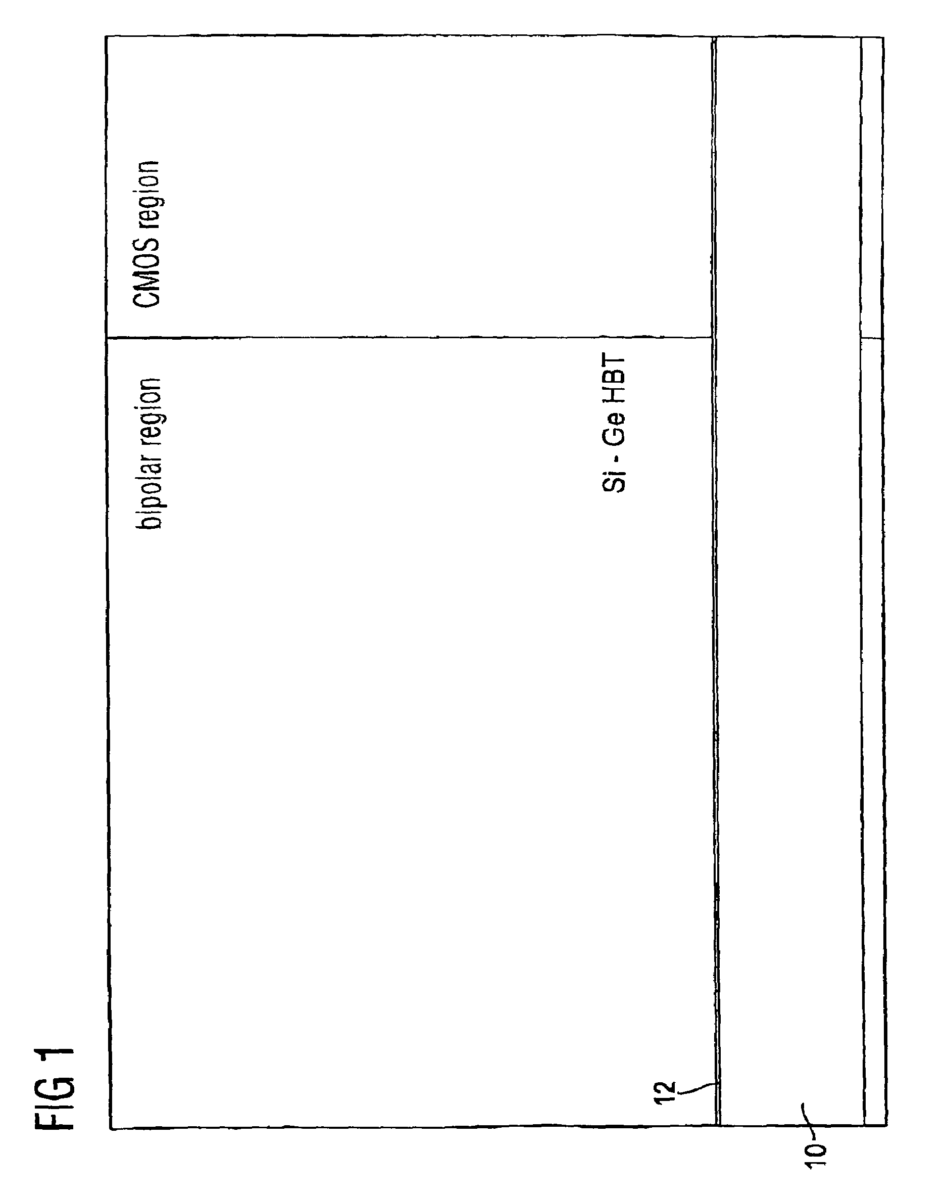
  • Figure 1
    Figure 1
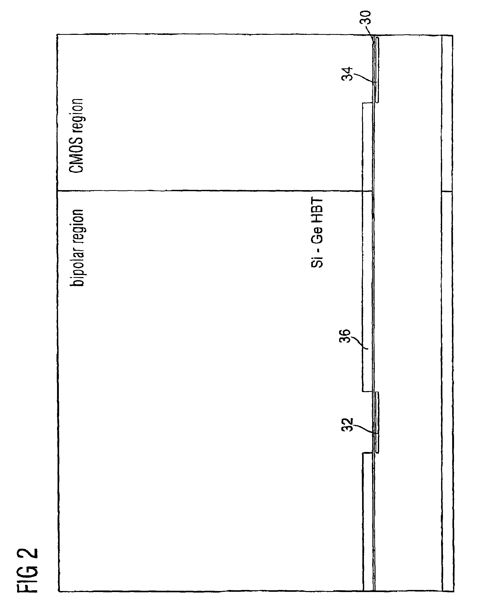
  • Figure 2
    Figure 2
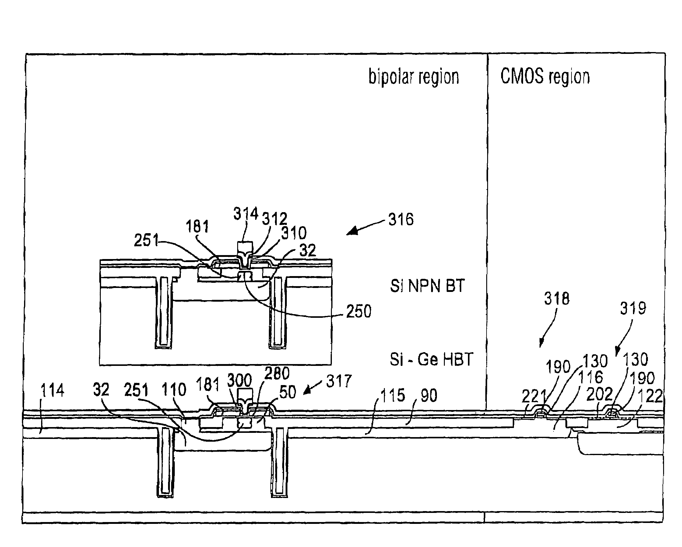
  • Figure 3
    Figure 3
Patent Text Reader

Abstract

For the integration of an npn bipolar transistor with a hetero bipolar transistor, a placeholder layer is generated in a base region of the hetero bipolar transistor after structuring a collector structure for both types of transistors, wherein the placeholder layer is not present in a base region of the bipolar transistor. After generating the base of the bipolar transistor, the base of the bipolar transistor is covered, whereupon the placeholder layer is removed and the base of the hetero bipolar transistor is generated in the places where the placeholder layer has been removed. The emitter structure is again generated equally for both types of transistors so that an integrated circuit results which includes bipolar transistors and hetero bipolar transistors whose collector structures and / or whose emitter structures consist of identical production layers. Thus, space-saving and cost-effective integrated circuits may be produced benefiting from the advantages of both types of transistors.
Need to check novelty before this filing date? Find Prior Art

Description

CROSS-REFERENCE TO RELATED APPLICATION

[0001] This application is a continuation of copending International Application No. PCT / EP03 / 05001, filed on May 13, 2003, which designated the United States and was not published in English.BACKGROUND OF THE INVENTION

[0002] 1. Field of the Invention

[0003] The present invention relates to integrated circuits and particularly to an integrated circuit including a bipolar transistor and a hetero bipolar transistor.

[0004] 2. Description of the Related Art

[0005] Bipolar transistors, i.e. transistors made of semiconductor material homogeneous with respect to the material, are known and include a collector, a base, and an emitter. In the case of an npn transistor, the collector is formed of an n-doped semiconductor material, the base is formed of a p-doped semiconductor material, and the emitter is formed of an n-doped semiconductor material.

[0006] A species of such an npn bipolar transistor (BT) is the so-called double poly-silicon bipolar transistor in se...

Examples

Embodiment Construction

[0050]Before the detailed process sequence for producing an inventive integrated circuit in accordance with a preferred embodiment, illustrated in FIGS. 1 to 26, is discussed in the following, the basic concept on which the present invention is based is explained with respect to FIG. 27. First, a semiconductor substrate for a common collector structure both for the bipolar transistor and the hetero bipolar transistor is structured (320). Next, the placeholder layer is generated in the base region of the hetero bipolar transistor, wherein, however, no placeholder layer is present in the base region of the bipolar transistor (322). Now, the base of the bipolar transistor and the collector of bipolar and hetero bipolar transistors are generated preferably by implanting and annealing with the placeholder layer of the hetero bipolar transistor in place. The placeholder layer ensures that the implantation atoms of the base implantation shot onto the integrated circuit do not penetrate the...