Method for manufacturing an integrated circuit and integrated circuit with a bipolar transistor and a hetero bipolar transistor

a technology of bipolar transistors and integrated circuits, applied in the field of integrated circuits, can solve the problems of higher chip area consumption, lower cut-off frequency, and more noise, and achieve the effects of low noise, high circuit yield, and good electric behavior

Inactive Publication Date: 2005-07-21
INFINEON TECH AG
View PDF13 Cites 3 Cited by
  • Summary
  • Abstract
  • Description
  • Claims
  • Application Information

AI Technical Summary

Benefits of technology

[0019] An advantage of the present invention is that now bipolar transistors may be integrated with HBTs in an integrated circuit in a cost-effective manner. Particularly for applications such as transmit / receive modules, in which characteristics of bipolar transistors and characteristics of hetero bipolar transistors are required at different locations, actually a hetero bipolar transistor may be used only at the location where it is necessarily required, while normal bipolar transistors may be used at other locations.
[0020] Overall, the circuit thus has a good electric behavior, because the low noise and the high cut-off frequency of the hetero bipolar transistors may be utilized, while, at the same time, the yield of the circuit is high, because only as few hetero bipolar transistors as possible are used so that the overall yield may be kept high, because the yield would decrease with an increasing number of hetero bipolar transistors on a circuit. On the other hand, chip area may be saved, because the good matching properties of the normal bipolar transistors may be utilized, namely also in those places in the circuit where it is actually necessary.
[0021] The inventive concept of the integration of bipolar transistors and hetero bipolar transistors in an integrated circuit, wherein both types of transistors are equal in their collector structure and / or their emitter structure, which is made possible by using the placeholder layer, may thus, on the one hand, generate a cost-effective circuit, which, on the other hand, has favorable electric properties dominated by the yield-critical and chip area-intensive hetero bipolar transistors where it is actually necessary. A further advantage of the present invention is that the integration concept for integrating bipolar transistors and hetero bipolar transistors is compatible with a CMOS process concept so that CMOS circuits may further be additionally integrated on the integrated circuit.

Problems solved by technology

The disadvantage of classic bipolar transistors compared to hetero bipolar transistors is the fact that they produce more noise than hetero bipolar transistors and that they have lower cut-off frequencies.
It is known from the integrated circuit technology that, in the case of a less favorable matching behavior, as it occurs in hetero bipolar transistors, this less favorable matching behavior may be compensated by increasing the overall size of the transistors, which results in a higher chip area consumption.
What is more important, however, is the disadvantage of the HBP that the yield, i.e. the number of functional transistors per waver, is significantly reduced compared to the yield with classic bipolar transistors.
The costs for a single module, however, increase with decreasing yield, so that a production of a transmit / receive module using classic bipolar transistors alone may have good yield and a low chip area consumption, but falls behind with respect to cut-off frequency and noise behavior compared to a complete implementation of the module with HBTs, while the HBT integration causes higher chip area consumption and lower yield, i.e. higher costs.

Method used


Image

  • Method for manufacturing an integrated circuit and integrated circuit with a bipolar transistor and a hetero bipolar transistor
  • Method for manufacturing an integrated circuit and integrated circuit with a bipolar transistor and a hetero bipolar transistor
  • Method for manufacturing an integrated circuit and integrated circuit with a bipolar transistor and a hetero bipolar transistor

Examples


Embodiment Construction

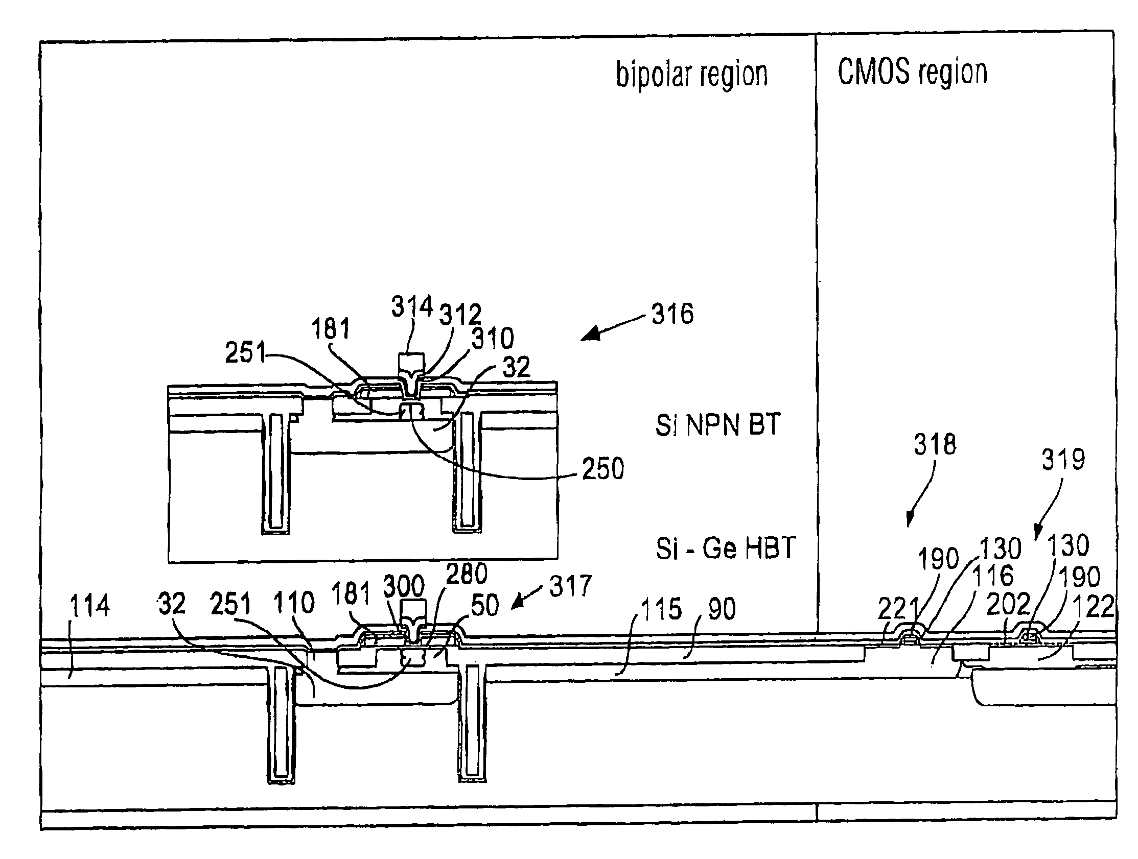
[0050] Before the detailed process sequence for producing an inventive integrated circuit in accordance with a preferred embodiment, illustrated in FIGS. 1 to 26, is discussed in the following, the basic concept on which the present invention is based is explained with respect to FIG. 27. First, a semiconductor substrate for a common collector structure both for the bipolar transistor and the hetero bipolar transistor is structured (320). Next, the placeholder layer is generated in the base region of the hetero bipolar transistor, wherein, however, no placeholder layer is present in the base region of the bipolar transistor (322). Now, the base of the bipolar transistor and the collector of bipolar and hetero bipolar transistors are generated preferably by implanting and annealing with the placeholder layer of the hetero bipolar transistor in place. The placeholder layer ensures that the implantation atoms of the base implantation shot onto the integrated circuit do not penetrate th...


PUM


Abstract

For the integration of an npn bipolar transistor with a hetero bipolar transistor, a placeholder layer is generated in a base region of the hetero bipolar transistor after structuring a collector structure for both types of transistors, wherein the placeholder layer is not present in a base region of the bipolar transistor. After generating the base of the bipolar transistor, the base of the bipolar transistor is covered, whereupon the placeholder layer is removed and the base of the hetero bipolar transistor is generated in the places where the placeholder layer has been removed. The emitter structure is again generated equally for both types of transistors so that an integrated circuit results which includes bipolar transistors and hetero bipolar transistors whose collector structures and/or whose emitter structures consist of identical production layers. Thus, space-saving and cost-effective integrated circuits may be produced benefiting from the advantages of both types of transistors.

Description

CROSS-REFERENCE TO RELATED APPLICATION [0001] This application is a continuation of copending International Application No. PCT / EP03 / 05001, filed on May 13, 2003, which designated the United States and was not published in English.BACKGROUND OF THE INVENTION [0002] 1. Field of the Invention [0003] The present invention relates to integrated circuits and particularly to an integrated circuit including a bipolar transistor and a hetero bipolar transistor. [0004] 2. Description of the Related Art [0005] Bipolar transistors, i.e. transistors made of semiconductor material homogeneous with respect to the material, are known and include a collector, a base, and an emitter. In the case of an npn transistor, the collector is formed of an n-doped semiconductor material, the base is formed of a p-doped semiconductor material, and the emitter is formed of an n-doped semiconductor material. [0006] A species of such an npn bipolar transistor (BT) is the so-called double poly-silicon bipolar tran...

Claims


Application Information

Patent Timeline
Patent Type & Authority Applications(United States)
IPC IPC(8): H01L21/8222H01L21/8249H01L27/06H01L27/082
CPCH01L21/8222H01L27/0825H01L27/0623H01L21/8249
Inventor DAHL, CLAUSMUELLER, KARL-HEINZWAGNER, CAJETAN
Owner INFINEON TECH AG
Why Eureka
Try Eureka