Metallization method of semiconductor device

a semiconductor device and contact technology, applied in semiconductor/solid-state device manufacturing, basic electric elements, electric devices, etc., can solve the problems of pvd sputtering generally having inferior step coverage ability, junction spiking, current leakage, etc., to improve barrier characteristics, superior step coverage and gap-filling properties

Inactive Publication Date: 2009-04-28
DONGBU ELECTRONICS CO LTD
View PDF3 Cites 0 Cited by
  • Summary
  • Abstract
  • Description
  • Claims
  • Application Information

AI Technical Summary

Benefits of technology

[0011]Consistent with the present invention, there is provided a method for forming a metallization contact in a semiconductor device. The metallization contact has a bilayer TiN structure having improved barrier characteristics against the diffusion of impurities. The bilayer TiN structure also enables superior step coverage and gap-fill properties in metal deposition.

Problems solved by technology

A significant problem in using aluminum for interconnects is junction spiking, which occurs at the interface of pure aluminum and silicon.
This problem worsens when the interface is heated during commonly performed heat treatments, such as annealing, due to the change of the solubility of silicon aluminum with temperature.
Junction spiking results in current leakage when the aluminum is a contact to a p-n junction.
However, PVD sputtering generally has inferior step coverage ability, and cannot provide adequate film thickness along the sidewalls of the contact hole.
Owing to the inferior step coverage, the electric resistivity of the metal wire increases during the operation of the device, resulting in decrease of the operational speed of the device, and over time, a short circuit condition between the active region of the substrate and the metal wire in the long run.
In addition, the inferior step coverage of PVD may disturb the subsequent deposition of aluminum or aluminum alloys in the contact hole.
As a result, subsequently deposited aluminum cannot provide sufficient coverage in the contact.
Most impurities can be removed by plasma treatment, but plasma ions cannot reach the lower part of the sidewalls of the contact hole.
As a result, contact resistance increases and device reliability decreases.

Method used


Image

  • Metallization method of semiconductor device
  • Metallization method of semiconductor device
  • Metallization method of semiconductor device

Examples


Embodiment Construction

[0020]Reference will now be made in detail to the present embodiments of the invention, examples of which are illustrated in the accompanying drawings. Wherever possible, the same reference numbers will be used throughout the drawings to refer to the same or like parts.

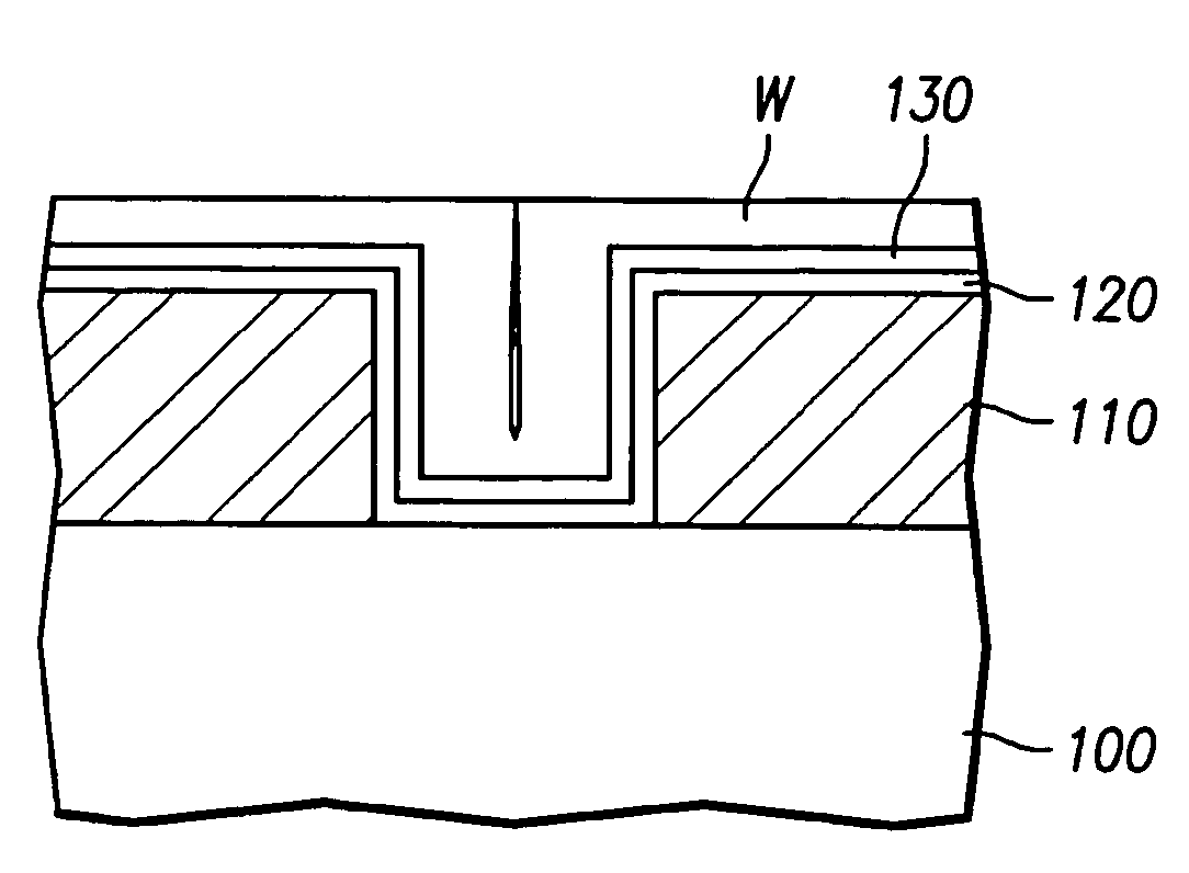
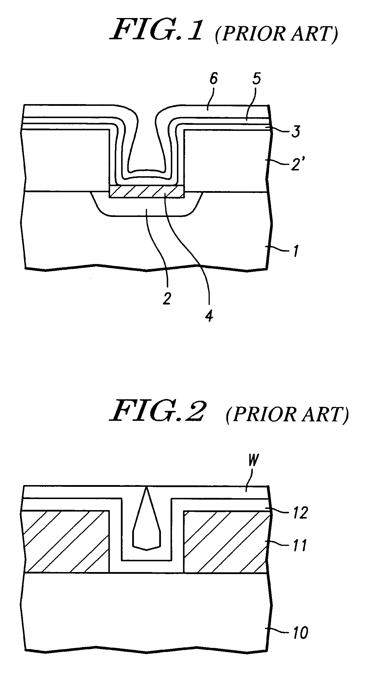
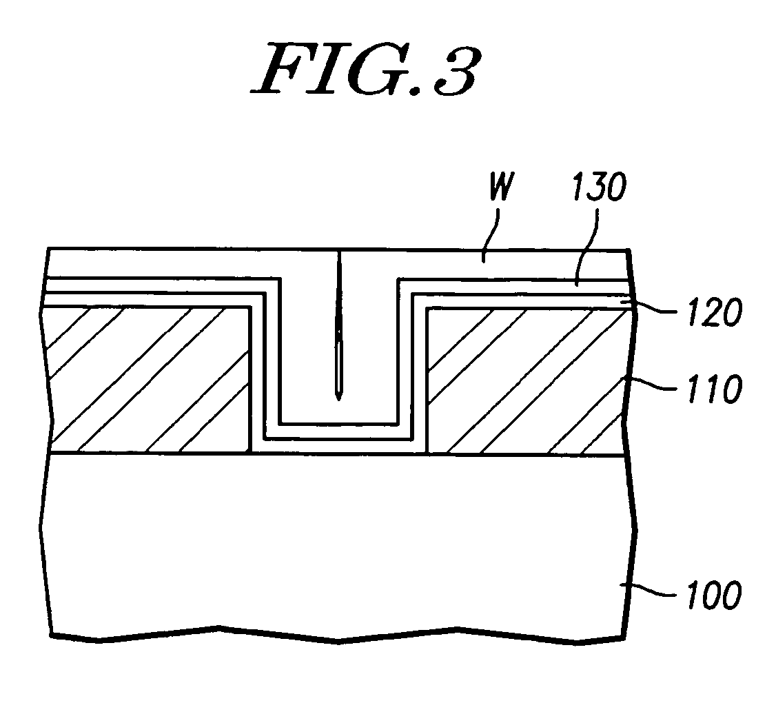
[0021]FIG. 3 illustrates an exemplary contact structure utilizing a bilayer TiN barrier structure with a tungsten contact layer. The bilayer TiN structure comprises two TiN layers having different densities deposited by PVD.

[0022]Referring to FIG. 3, a contact hole (or via hole, not numbered) is formed by etching a predetermined portion of an insulating layer 110 formed on a silicon substrate 100. The contact hole exposes a portion of an active region of substrate 100. TiN layers 120 and 130 are then formed over the entire surface of substrate 100 by PVD process using ionized metal plasma (IMP) and a mixed gas of nitrogen (N2) and argon (Ar).

[0023]Before the formation of TiN layers 120 and 130, a Ti layer can be first...


PUM


Abstract

A method for forming a metallization contact in a semiconductor device includes (a) forming an insulating layer on a semiconductor substrate including an active device region or a lower metal wire; (b) forming a contact hole to expose a portion of the active device region or lower metal wire by etching a portion of the insulating layer; (c) depositing a first TiN layer on the insulating layer and inside the contact hole by a PVD process using a first carrier gas composition of nitrogen (N2) and argon (Ar); (d) depositing a second TiN layer on the first TiN layer by a PVD process using a second carrier gas composition of nitrogen (N2) and argon (Ar); and (e) forming a metal layer on the second TiN layer.

Description

[0001]This application claims the benefit of priority of Korean Application No. 10-2004-0117695, filed on Dec. 31, 2004, which is incorporated by reference herein in its entirety.BACKGROUND OF THE INVENTION[0002]1. Field of the Invention[0003]The present invention relates generally to semiconductor device manufacturing technology, and particularly to a method for forming a metallization contact in a semiconductor device.[0004]2. Description of the Related Art[0005]Thin film aluminum and aluminum alloys are fundamental materials having application in the semiconductor integrated circuits industry. Aluminum is a good conductor, and adheres well to silicon and silicon dioxide. A significant problem in using aluminum for interconnects is junction spiking, which occurs at the interface of pure aluminum and silicon. This problem worsens when the interface is heated during commonly performed heat treatments, such as annealing, due to the change of the solubility of silicon aluminum with te...

Claims


Application Information

Patent Timeline
Patent Type & Authority Patents(United States)
IPC IPC(8): H01L21/44
CPCH01L21/2855H01L21/76843H01L21/76846H01L21/28
Inventor KIM, JUNG JOO
Owner DONGBU ELECTRONICS CO LTD
Why Eureka
Try Eureka