CMOS active pixel sensor and active pixel sensor array using fingered type source follower transistor

a technology of active pixel sensor and source follower transistor, which is applied in the field of complementary metaloxide semiconductor (cmos) active pixel sensor, can solve the problems of manufacturing cost and power consumption, disadvantages of ccd type, and difficulty in maintaining the image quality of pixel sensor beyond a predetermined image quality

Active Publication Date: 2009-04-28
SAMSUNG ELECTRONICS CO LTD
View PDF14 Cites 40 Cited by
  • Summary
  • Abstract
  • Description
  • Claims
  • Application Information

AI Technical Summary

Benefits of technology

[0108]While the example embodiments of the present disclosure and their advantages have been described in detail, it shall be understood that various changes, substitutions and alterations may be made herein by those of ordinary skill in the pertinent art without departing from the scope of the invention.

Problems solved by technology

In addition, the CCD type has disadvantages, with respect to manufacturing costs and power consumption, compared with the CMOS type.
In addition, as the pixel size decreases, it is difficult to maintain the image quality of the pixel sensor beyond a predetermined image quality.
In particular, the CMOS active pixel sensor is restricted to an optically symmetrical structure due to the characteristics of the CMOS active pixel sensor and the decreasing sizes of the transistors in the pixel, so that the CMOS active pixel sensor is very vulnerable to noise.

Method used


Image

  • CMOS active pixel sensor and active pixel sensor array using fingered type source follower transistor
  • CMOS active pixel sensor and active pixel sensor array using fingered type source follower transistor
  • CMOS active pixel sensor and active pixel sensor array using fingered type source follower transistor

Examples


Embodiment Construction

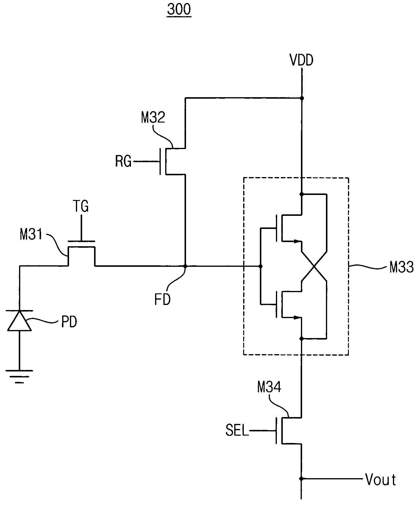
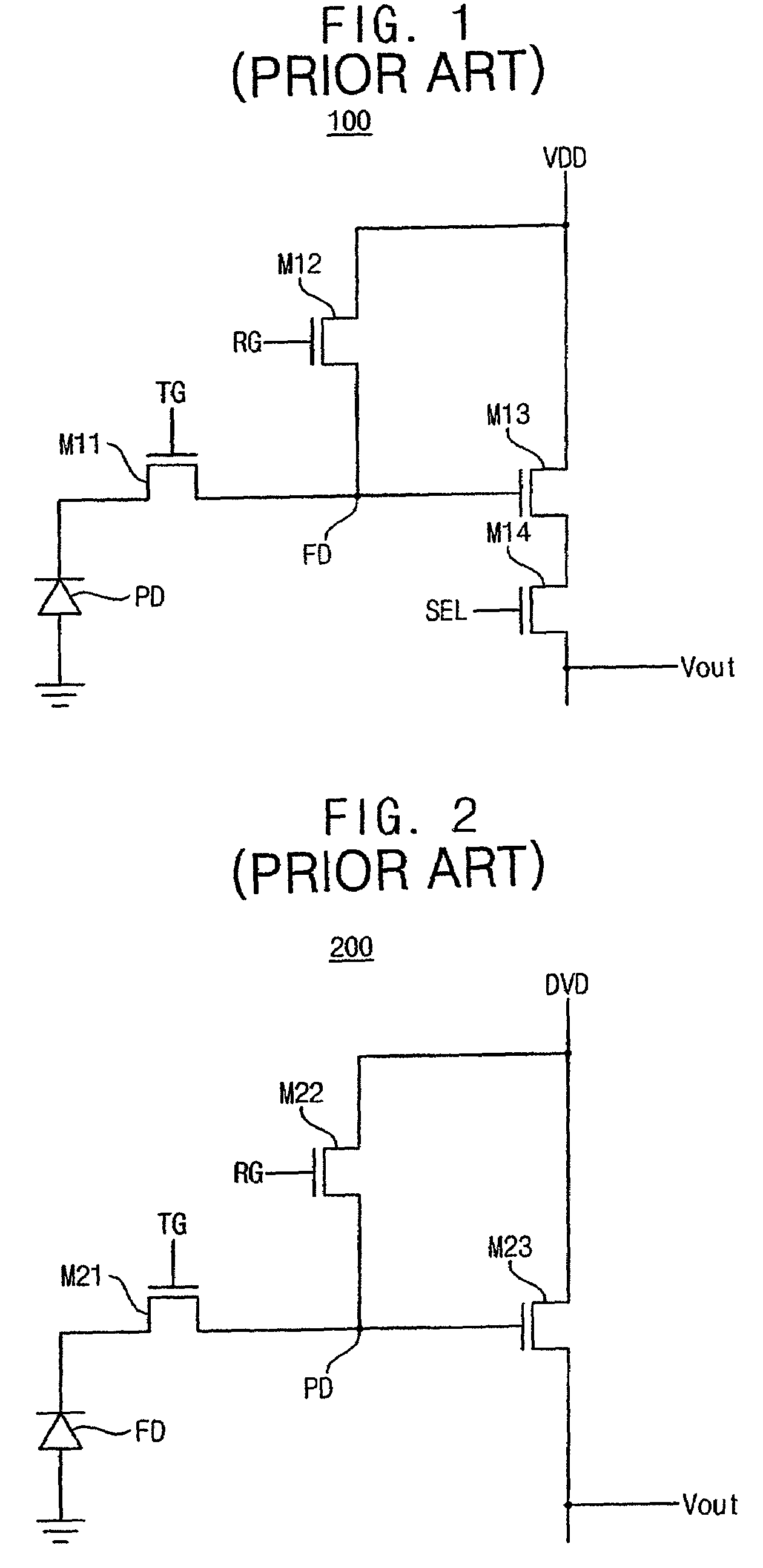
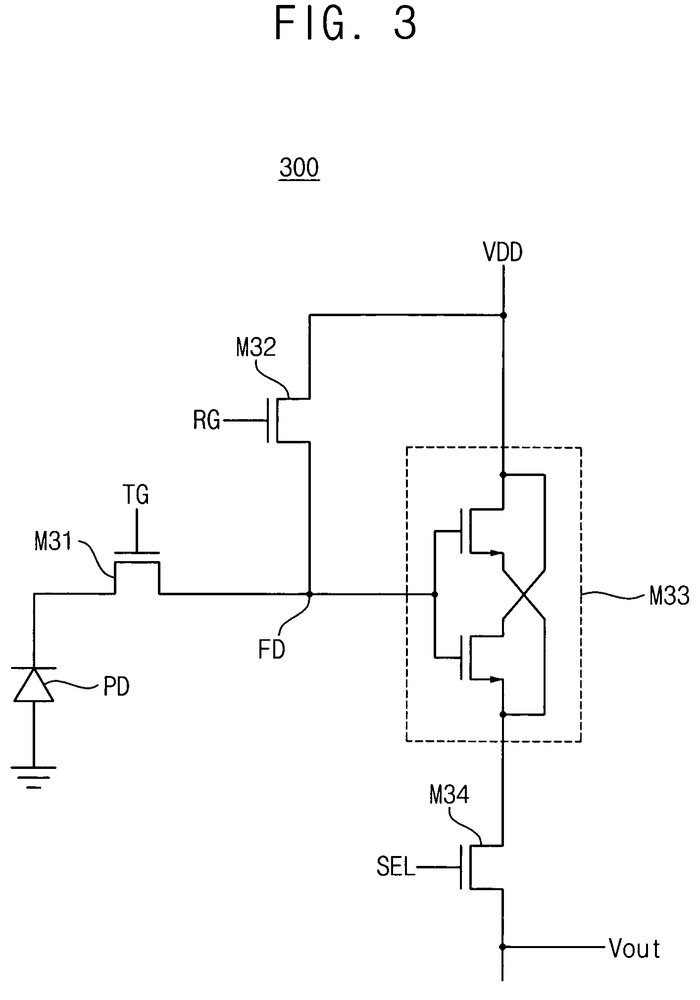
[0048]Example embodiments of the present disclosure provide for a Complementary Metal-Oxide Semiconductor (CMOS) active pixel sensor having a fingered type source follower transistor and reduced device noise. It shall be understood that specific structural and functional details disclosed herein are merely representative for purposes of describing example embodiments of the present disclosure; in addition, example embodiments of the present disclosure may be embodied in many alternate forms and should not be construed as limited to example embodiments of the present disclosure set forth herein.

[0049]Accordingly, while the invention is susceptible to various modifications and alternative forms, specific embodiments thereof are shown by way of example in the drawings and will herein be described in detail. It should be understood, in addition, that there is no intent to limit the invention to the particular forms disclosed, but on the contrary, all modifications, equivalents, and alte...


PUM


Abstract

A CMOS active pixel sensor includes a photodiode, a transmitting transistor, a reset transistor, a fingered type source follower transistor and a selecting transistor, where the photodiode generates charge in response to incident light, the transmitting transistor transmits the charge stored in the photodiode to a sensing node, the reset transistor, coupled to a power supply voltage, resets a voltage of the sensing node so that the sensing node has substantially a level of the power supply voltage, the fingered type source follower transistor amplifies the voltage of the sensing node, the selecting transistor transmits a voltage of a source electrode of the fingered type source follower transistor into an internal circuit in response to a selection signal, thus, the channel width of the source follower transistor may be increased, and the MOS device noise due to the source follower transistor may be reduced.

Description

CROSS-REFERENCE TO RELATED APPLICATION[0001]This application claims foreign priority under 35 U.S.C. § 119 to Korean Patent Application No. 2005-11126 filed on Feb. 7, 2005 in the Korean Intellectual Property Office (KIPO), the entire contents of which are hereby incorporated by reference.BACKGROUND[0002]1. Field of the Invention[0003]The present disclosure relates to active pixel sensors, and more particularly to Complementary Metal-Oxide Semiconductor (CMOS) active pixel sensors.[0004]2. Description of the Related Art[0005]An Active Pixel Sensor (APS) converts a photo image into an electrical signal, and is widely used in digital cameras, mobile phones having a camera, vision systems, and the like.[0006]Active pixel sensors are classified into a Charge-Coupled Device (CCD) type and a Complementary Metal-Oxide Semiconductor (CMOS) type. The CCD type has less noise than the CMOS type and has better image quality than the CMOS type. In addition, the CCD type has disadvantages, with r...

Claims


Application Information

Patent Timeline
Patent Type & Authority Patents(United States)
IPC IPC(8): H01L27/00H01L31/062H04N5/359H04N5/361H04N5/363H04N5/374
CPCH01L27/14603A61B1/00016G06T5/50G06F3/00
Inventor KIM, YOUNG-CHANKIM, YI-TAE
Owner SAMSUNG ELECTRONICS CO LTD
Why Eureka
Try Eureka