Liquid crystal display device and electronic apparatus

a liquid crystal display device and electronic equipment technology, applied in non-linear optics, instruments, optics, etc., can solve the problems of difficult to form step differences, lack of freedom in optical design, and drawbacks of reflective liquid crystal display devices in the related art, so as to improve contrast, improve contrast, and improve contrast

Active Publication Date: 2009-05-05
BOE TECH GRP CO LTD
View PDF13 Cites 6 Cited by
  • Summary
  • Abstract
  • Description
  • Claims
  • Application Information

AI Technical Summary

Benefits of technology

[0013]An advantage of the invention is that it provides a transflective liquid crystal display device having high contrast while retaining the benefit of the vertical alignment mode, such as a wide viewing angle.
[0014]According to an aspect of the invention, a liquid crystal display device of the invention includes: a pair of substrates including an element substrate and a counter substrate; a liquid crystal layer interposed between the pair of substrates, the liquid crystal layer being composed of liquid crystal having negative dielectric anisotropy, an initial alignment state thereof being vertical; pixel electrodes provided on the element substrate to drive the liquid crystal layer; and a transmissive display region for transmissive display and a reflective display region for reflective display provided within one dot region. Also, at least an outer region of the pixel electrodes and a region overlapping edges of the pixel electrodes in plan view become the reflective display region, and the thickness of the liquid crystal layer in the reflective display region is approximately equal to that of the liquid crystal layer in the transmissive display region.
[0015]The liquid crystal display device of the invention is achieved by combining the transflective liquid crystal display device and liquid crystal in the vertical alignment mode. As described previously, in order to overcome a problem of deterioration of contrast due to a difference in retardation between the reflective mode and the transmissive mode in recent transflective liquid crystal display devices, there has been suggested the so-called multi-gap structure in which the thickness of the liquid crystal layer in the reflective display region and the transmissive display region is modified by, for example, making the resin layer having a predetermined thickness in the reflective display region on the substrate protruding toward the liquid crystal layer. Various applications in connection with this kind of liquid crystal display device have been already filed by the applicant. With this configuration, since the thickness of the liquid crystal layer in the reflective display region can be smaller than the thickness of the liquid crystal layer in the transmissive display region due to the existence of the resin layer, the retardation in the reflective display can become approximately equal to the retardation in the transmissive display, which theoretically results in improvement of contrast. However, in actuality, deterioration of contrast occurred due to the slope of the resin layer.
[0016]So, in consideration of the above, the inventors paid attention to an aspect that different retardations necessarily occur within one dot region in a liquid crystal display. device of a vertical alignment mode even though the multi-gap structure is not employed. That is, in an active-matrix-type liquid crystal display device having one pixel electrode within one dot region, since an electric field is not applied to a region between adjacent pixel electrodes, liquid crystal molecules do not fall down in these regions. On the other hand, in the middle region of the pixel electrode, the liquid crystal molecules fall down in a horizontal direction when the electric field is applied. Further, in an edge of the pixel electrode, which is an intermediate region between the region between adjacent pixel electrodes and the middle region of the pixel electrode, since the electric field is applied to the liquid crystal layer in a direction inclined from the normal line direction of the substrate surface, the liquid crystal molecules fall down halfway. Accordingly, the retardation continues to become small from the middle region of the pixel electrode to the edge of the pixel electrode 9 and then the region between adjacent electrodes (an outer side of the pixel electrode). Accordingly, by using an outer region of the pixel electrode and a region corresponding to the edge of the pixel electrode as the reflective display region and using other remaining regions as the transmissive display region, the retardation in the reflective display region can be smaller than the retardation in the transmissive display region without employing the multi-gap structure, thereby improving contrast in both of the reflective display and transmissive display. With this configuration, since an adverse effect caused by the resin layer in the multi-gap structure can be eliminated, a liquid crystal display device having high contrast can be realized.
[0017]In the above configuration of the invention, preferably, an alignment controller that controls an alignment direction of the liquid crystal layer is further provided in a region of the counter substrate which overlaps the pixel electrodes in plan view. The alignment controller may include an opening formed in an electrode or a convex portion (protrusion) formed on an electrode.
[0018]As described above, since the electric field applied to the liquid crystal layer at the edge of the pixel electrode in the direction inclined with respect to the normal line direction of the substrate can drop the liquid crystal molecules down in a radial direction, it is possible to control. the direction of alignment. However, since this electric field does not necessarily provide a sufficient alignment control, the alignment control can be further intensified by forming the alignment controller at a position on the counter substrate corresponding to the middle region of the pixel electrode, for example. As a result, an alignment division structure can be reliably implemented, thereby obtaining the wide viewing angle.

Problems solved by technology

However, the transflective liquid crystal display device in the related art has a drawback due to a narrow viewing angle in the transmissive mode.
This disadvantage results from the lack of freedom in optical design with the restriction that the reflective display has to be achieved by a single polarization plate provided at a viewer side because a transflective plate is provided on an inner side of a liquid crystal cell so that parallax does not occur.
However, when realizing such a structure within a liquid crystal cell, it is difficult to form the step difference and to prevent a slope (an inclined portion) of the resin layer from being generated at a boundary between the transmissive display region and the reflective display region.
For this reason, the liquid crystal located at the slope of the resin layer is aligned obliquely with respect to a substrate surface although it is in a vertical alignment mode, which causes deterioration of display contrast.
However, in actuality, deterioration of contrast occurred due to the slope of the resin layer.
However, since this electric field does not necessarily provide a sufficient alignment control, the alignment control can be further intensified by forming the alignment controller at a position on the counter substrate corresponding to the middle region of the pixel electrode, for example.
However, since this electric field does not necessarily provide a sufficient alignment control, the alignment control can be further intensified by forming the alignment controller at a position on the counter substrate corresponding to the middle region of the island-shaped portions, for example.

Method used


Image

  • Liquid crystal display device and electronic apparatus
  • Liquid crystal display device and electronic apparatus
  • Liquid crystal display device and electronic apparatus

Examples


first embodiment

[0044]Hereinafter, a first embodiment of the invention will be described with reference to FIGS. 1 to 3.

[0045]A liquid crystal display device according to this embodiment is an example of an active-matrix-type liquid crystal display device using a thin film transistor (TFT) as a switching element.

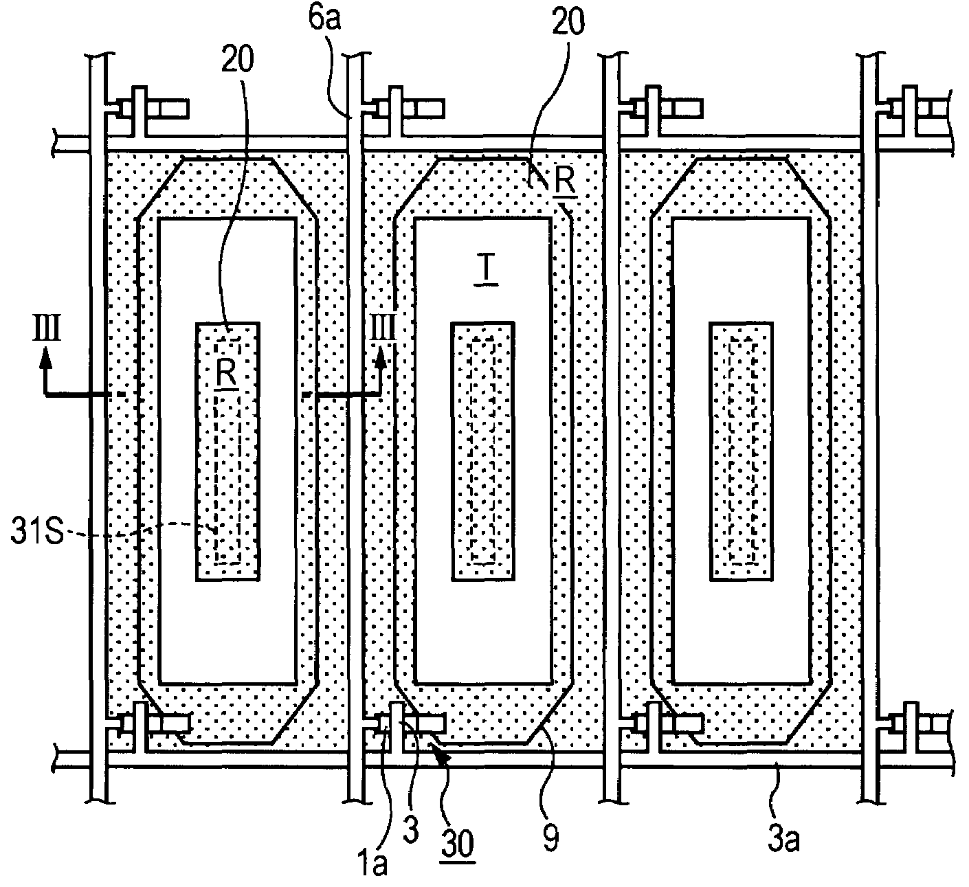
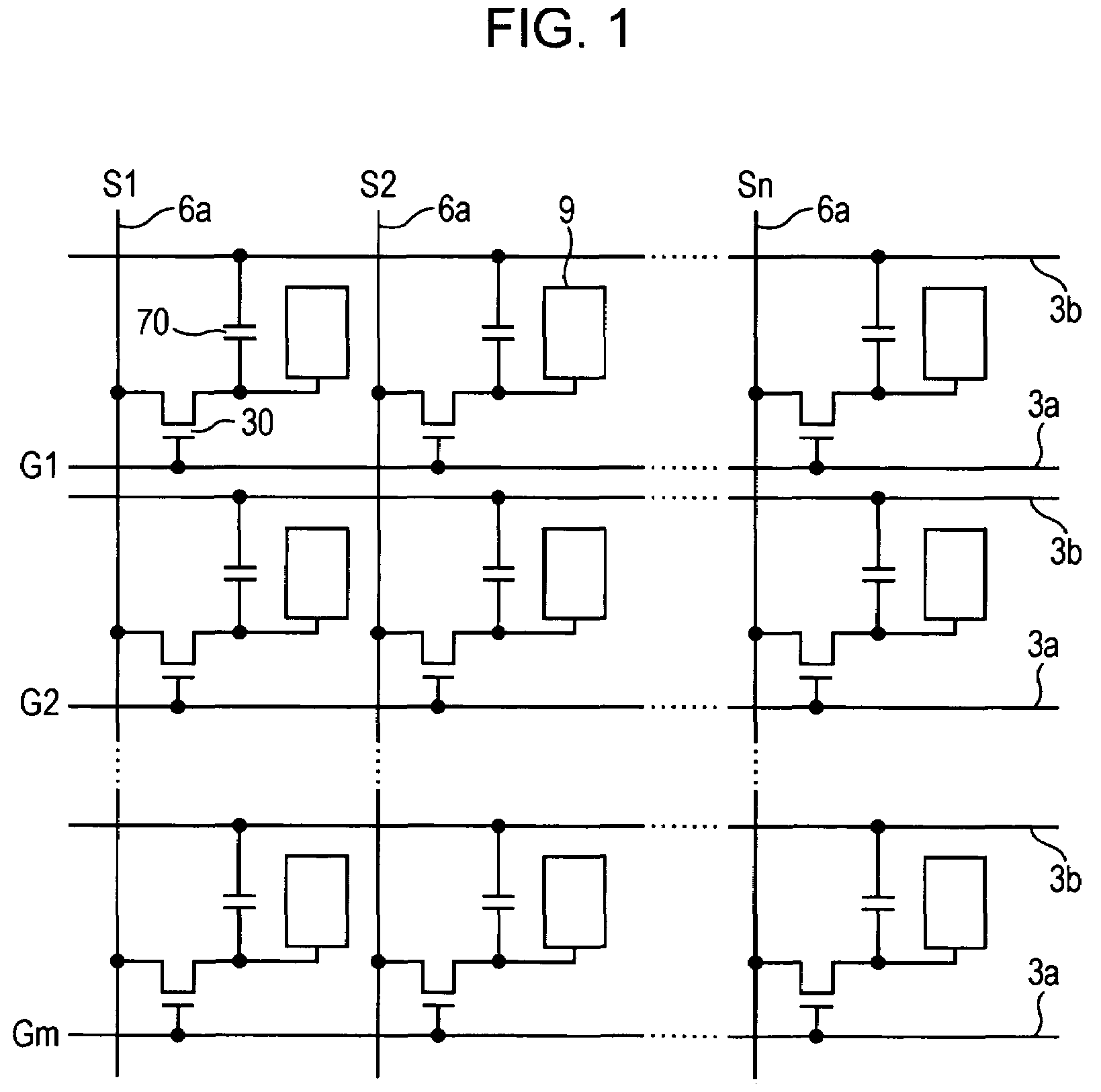
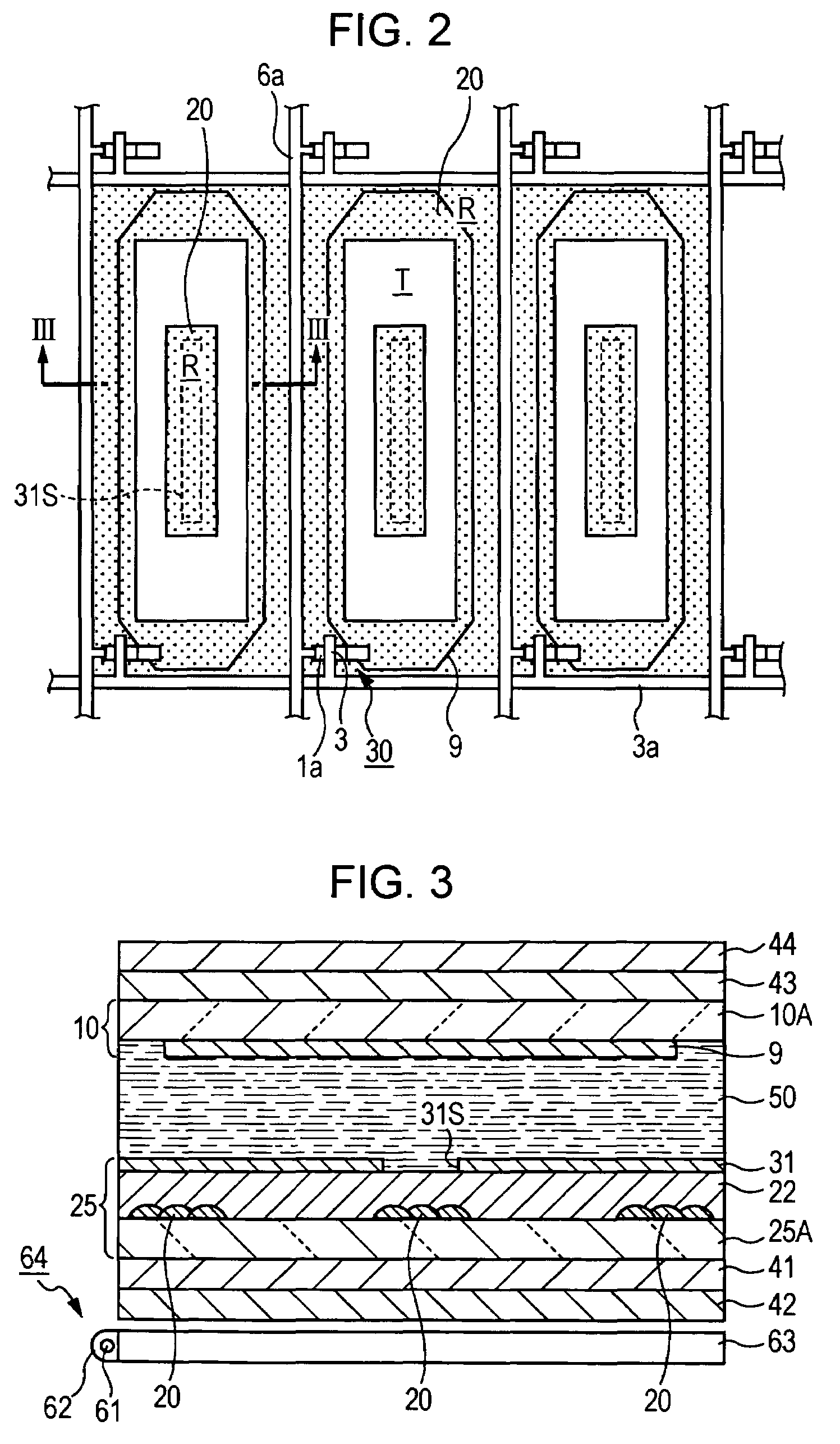
[0046]FIG. 1 is an equivalent circuit diagram showing a plurality of dots, which are arranged in a matrix, constituting an image display region of the liquid crystal display device according the embodiment, FIG. 2 is a plan view showing a structure within a dot region of a TFT array substrate, FIG. 3 is a cross-sectional view, which is taken along line III-III of FIG. 2, showing a structure of the liquid crystal display device, and FIG. 4 is a view showing an alignment state of liquid crystal molecules. Throughout the drawings, the scale of each layer of member is adjusted in order to have a recognizable size in the drawings.

[0047]As shown in FIG. 1, for the liquid crystal display device ac...

second embodiment

[0064]Hereinafter, a second embodiment of the invention will be described with reference to FIGS. 5 and 6.

[0065]FIG. 5 is a cross-sectional view of a liquid crystal display device according to a second embodiment of the invention, and FIG. 6 is a view showing an alignment state of liquid crystal. The liquid crystal display device according to the embodiment has the same basic configuration as the first embodiment. Therefore, in FIGS. 5 and 6, the same elements as in FIGS. 3 and 4 are denoted by the same reference numerals and detailed explanation thereof will be omitted for the sake of simplicity.

[0066]In this embodiment, a convex portion 29 (alignment controller) having a triangular cross section is formed on the common electrode 31 located at the counter substrate 25 side, as shown in FIG. 5, instead of the opening 31S of the common electrode 31. The convex portion 29 is made of a dielectric material such as an acryl resin or the like and has a planar shape linearly formed in the ...

third embodiment

[0069]Hereinafter, a third embodiment of the invention will be described with reference to FIGS. 7 to 9.

[0070]FIG. 7 is a plan view showing configuration of dot regions of a liquid crystal display device according to the embodiment, FIG. 8 is a cross-sectional view taken along line VIII-VIII of FIG. 7, showing the configuration of the liquid crystal display device of the third embodiment, and FIG. 9 is a view showing an alignment state of liquid crystal when a selective voltage is applied. The liquid crystal display device according to the embodiment has the same basic configuration as the first embodiment. Therefore, in FIGS. 7 to 9, the same elements as in FIGS. 2 to 4 are denoted by the same reference numerals and detailed explanation thereof will be omitted for the sake of simplicity.

[0071]In the third embodiment, as shown in FIG. 7, the pixel electrode 9 is configured to include three island-shaped portions 9a, 9b, and 9c. The three island-shaped portions 9a, 9b, and 9c are ele...


PUM

PropertyMeasurementUnit
dielectric anisotropyaaaaaaaaaa
thicknessaaaaaaaaaa
voltageaaaaaaaaaa

Abstract

A liquid crystal display device includes: a pair of substrates including an element substrate and a counter substrate; a liquid crystal layer interposed between the pair of substrates, the liquid crystal layer being composed of liquid crystal having negative dielectric anisotropy, an initial alignment state thereof being vertical; pixel electrodes provided on the element substrate to drive the liquid crystal layer; and a transmissive display region for transmissive display and a reflective display region for reflective display provided within one dot region. At least an outer region of the pixel electrodes and a region overlapping edges of the pixel electrodes in plan view become the reflective display region, and the thickness of the liquid crystal layer in the reflective display region is approximately equal to that of the liquid crystal layer in the transmissive display region.

Description

RELATED APPLICAATIONS[0001]This application claims priority to Japanese Patenet Application No. 2004-262272 filed Sep. 9, 2004 which is hereby expressly incorporated by reference herein in its entirety.BACKGROUND OF THE INVENTION[0002]1. Technical Field[0003]The present invention relates to a liquid crystal display device and an electronic apparatus, and in particular, to a technique capable of realizing high contrast and wide viewing angle in a transflective liquid crystal display device having both reflective and transmissive modes.[0004]2. Related Art[0005]There has been suggested a liquid crystal display device in which images can be viewed by using external light in a bright place, as in a reflective liquid crystal display device, and by using an internal light source, such as a backlight or the like, in a dark place. Such a liquid crystal display device employing both reflective and transmissive modes switches between both the modes depending on the ambient brightness. This al...

Claims


Application Information

Patent Timeline
Patent Type & Authority Patents(United States)
IPC IPC(8): G02F1/1335
CPCG02F1/133555G02F1/1393G02F1/1337
Inventor TSUCHIYA, HITOSHI
Owner BOE TECH GRP CO LTD
Why Eureka
Try Eureka