Semiconductor device including back-gated transistors and method of fabricating the device

a technology of backgated transistors and semiconductor devices, which is applied in semiconductor devices, digital storage, instruments, etc., can solve the problems of affecting sram devices, vt control becomes more difficult, and dopant fluctuations become serious problems in vt control

Active Publication Date: 2009-05-12
GLOBALFOUNDRIES U S INC
View PDF9 Cites 29 Cited by
  • Summary
  • Abstract
  • Description
  • Claims
  • Application Information

AI Technical Summary

Benefits of technology

[0008]In addition, present invention may help to increase the device density of the novel semiconductor structure. The present invention may also improve the stability of a device (e.g., an SRAM device) by coupling the back-gates of the proper nFET devices in the SRAM. In addition, the present invention may be used to apply a proper biasing condition.

Problems solved by technology

In advanced semiconductor devices (e.g., such as the conventional SRAM device 100), dopant fluctuations are becoming a serious problem in Vt (threshold voltage) control.
As semiconductor devices become smaller and smaller, Vt control becomes more difficult.
This problem greatly affects SRAM devices since the SRAM devices may be very small.
One serious problem with this solution, however, is that the use of back-gates in semiconductor devices results in increased layout complexity, and therefore, higher cost.
In addition, separately back gating the individual devices increases wiring densities and does not help in the layout compactness.

Method used


Image

  • Semiconductor device including back-gated transistors and method of fabricating the device
  • Semiconductor device including back-gated transistors and method of fabricating the device
  • Semiconductor device including back-gated transistors and method of fabricating the device

Examples


Embodiment Construction

[0032]Referring now to the drawings, FIGS. 2-13H illustrate the exemplary aspects of the present invention.

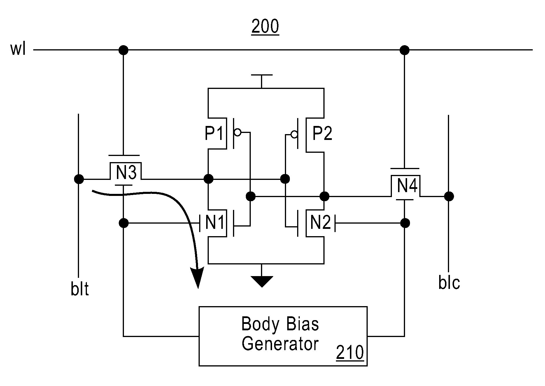
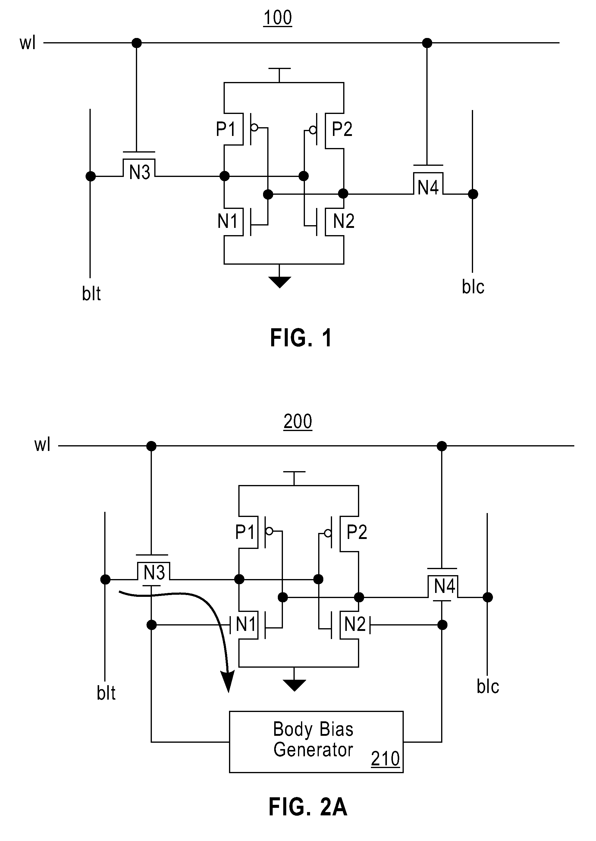
[0033]The present invention provides a compact, coupled backgating structure for a static random access memory (SRAM) device.

[0034]Referring again to FIG. 1, the inventors have recognized that by coupling the gates in the SRAM device (e.g., coupling the gates in the form of a finFET) the layout complexities can be reduced. In addition, the inventors have recognized that a forward bias that is larger than Vdd (e.g., a larger-than Vdd scheme) may help to improve the delay (e.g., in an active mode), while a reverse bias may lower the leakages of the SRAM cells in standby mode.

[0035]FIG. 2A provides a circuit diagram illustrating a memory cell 200 (e.g., a 6-T SRAM finFET cell) according to the exemplary aspects of the present invention. The pFETs (e.g., P1, P2) can be operating in double-gate mode, and the back-gates of the nFETs N1, N3 (e.g., as a pair) and nFETs N2, N4 (e.g., as...


PUM


Abstract

A memory cell (e.g., static random access memory (SRAM) cell) includes a plurality of back-gated n-type field effect transistors (nFETs), and a plurality of double-gated p-type field effect transistors (pFETs) operatively coupled to the plurality of nFETs.

Description

BACKGROUND OF THE INVENTION[0001]1. Field of the Invention[0002]The present invention relates to a semiconductor device (e.g., a static random access memory (SRAM) device) including back-gated transistors, and more particularly, to a device which includes a back-gate transistor which may be fabricated using finFET technologies (e.g., a coupled backgate finFET SRAM).[0003]2. Description of the Related Art[0004]FIG. 1 provides a circuit diagram illustrating a conventional six transistor (6-T) SRAM device 100. As illustrated in FIG. 1, the conventional SRAM device 100 includes n-type field effect transistors (nFETs) N1-N4, and p-type field effect transistors (pFETs) P1-P2. The word line (wl) is coupled to the gates of nFETs N3, N4 and the bit lines blt, blc are coupled to an arm of nFETs N3, N4, respectively.[0005]In advanced semiconductor devices (e.g., such as the conventional SRAM device 100), dopant fluctuations are becoming a serious problem in Vt (threshold voltage) control. As s...

Claims


Application Information

Patent Timeline
Patent Type & Authority Patents(United States)
IPC IPC(8): G11C11/00
CPCH01L27/1104G11C11/412H01L27/0207H01L27/11H01L29/66795H01L29/785H10B10/00H10B10/12
Inventor JOSHI, RAJIV V.KIM, KEUNWOONOWAK, EDWARD JOSEPHWILLIAMS, RICHARD QUIMBY
Owner GLOBALFOUNDRIES U S INC
Why Eureka
Try Eureka