Device and method for manufacturing the same

a technology of manufacturing method and device, applied in the direction of resistors, non-adjustable resistors, using electrical/magnetic means, etc., can solve the problems of reducing connection reliability, reducing the reliability of components having such small dimensions, and affecting the normal operation of the automatic population

Active Publication Date: 2009-05-26
SENSOTHERM TEMPERATURSENSORIK
View PDF25 Cites 3 Cited by
  • Summary
  • Abstract
  • Description
  • Claims
  • Application Information

AI Technical Summary

Benefits of technology

[0012]Starting from this prior art, it is an object of the present invention to provide an enhanced method for manufacturing a device and an enhanced device, which enables to handle and to contact a component securely and reliably despite its small dimension.

Problems solved by technology

The situation is different when the devices used are used in a number not enabling strapped arrangement of the components and also no automatic population.
Due to the many varying locations of employment of such sensor devices, automated population does usually not make sense.
The above-described advantages regarding material yield and the like, which are obtained by the further miniaturization, lead, however, in connection with the handling of individual temperature sensors, to all new problems as a counter-move, in particular regarding the durability of such components and the contacting capacity of such components.
More specifically, it is obvious that components having such small dimensions are only difficult to handle since those are only difficult to grip and to place.
A further problem occurs when the components are not soldered, but are for example to be contacted with a lead wire.
It is obvious that with device dimensions becoming ever smaller also the areas available for the attachment of a lead wire become ever smaller, so that here, to be consistent, a reduction in the adhesion forces results, which in the end leads to reduced connection reliability.

Method used


Image

  • Device and method for manufacturing the same
  • Device and method for manufacturing the same
  • Device and method for manufacturing the same

Examples


Embodiment Construction

[0032]Regarding the following description of the preferred embodiments, it is pointed out that in the appended drawings like or similar elements are provided with like reference numerals.

[0033]On the basis of FIG. 1 to FIG. 5, a preferred embodiment of the inventive manufacturing method is now explained in greater detail on the basis of temperature sensors.

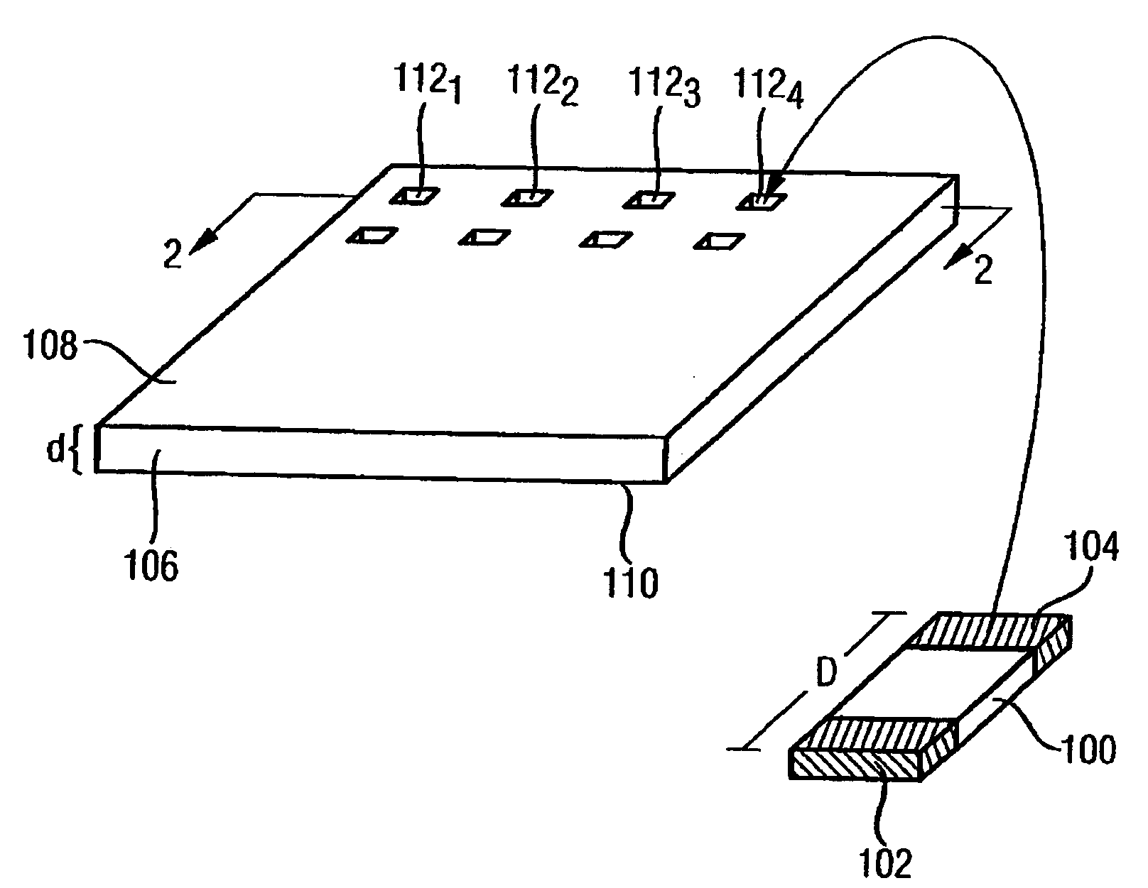
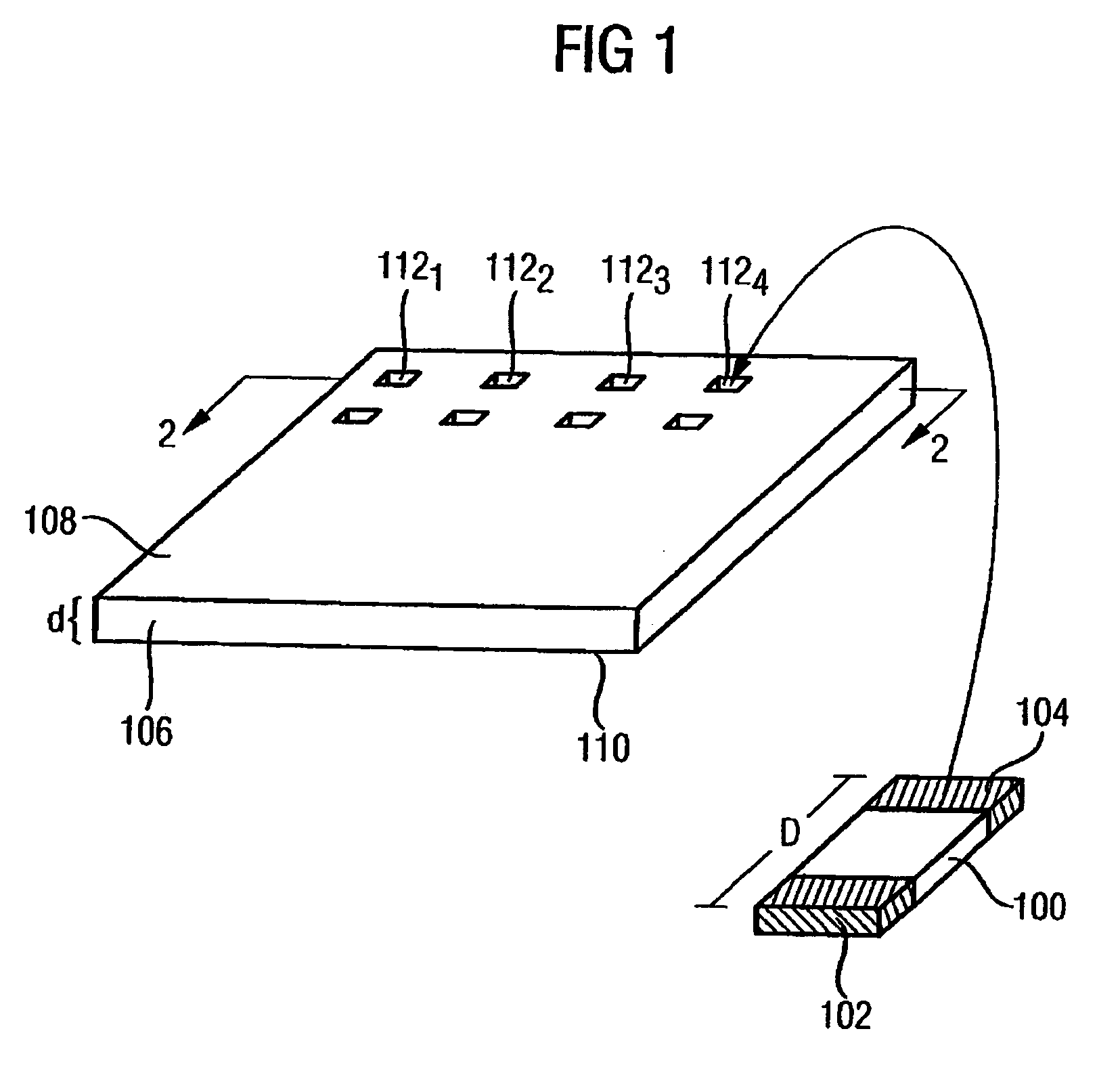
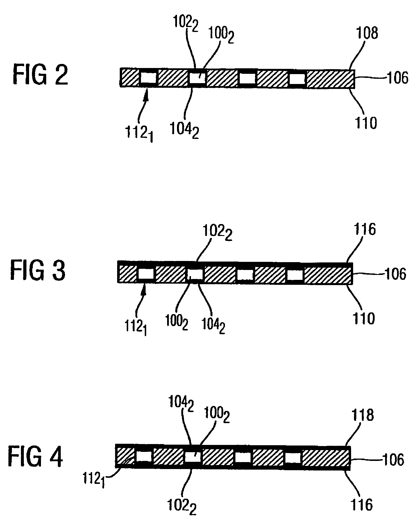
[0034]In FIG. 1, a SMD temperature sensor 100 is shown, which has a first terminal region 102 and a second terminal region 104. The SMD temperature sensor shown has a longitudinal dimension D, as this is shown in FIG. 1. Although the preferred embodiment is described on the basis of SMD temperature sensors, it is to be noted that the present invention is not limited hereto, but rather finds application with arbitrary components having at least one terminal region.

[0035]In a first step, a plurality of SMD temperature sensors 100 are provided, which were manufactured conventionally, for example. The SMD device 100 is, for example, a...


PUM

PropertyMeasurementUnit
conductiveaaaaaaaaaa
dimensionaaaaaaaaaa
non-conductiveaaaaaaaaaa

Abstract

In a method for manufacturing a device, at first a plurality of components each having at least a first terminal region are provided. Furthermore, a support with a first surface, in which a plurality of recesses are formed, is provided. The components provided are inserted into the recesses such that the first terminal region of each component faces the first surface of the support. Conductive material is applied on the first surface of the support such that the conductive material is in contact with the first terminal region of each component. Finally, the support is diced to obtain the individual devices.

Description

CROSS-REFERENCE TO RELATED APPLICATION[0001]This application is a continuation of co-pending International application No. PCT / EP2004 / 013384, filed Nov. 25, 2004, which designated the United States and was not published in English and is incorporated herein by reference in its entirety.BACKGROUND OF THE INVENTION[0002]1. Field of the Invention[0003]The present invention relates to a device and to a method for manufacturing the same, and here in particular to a device having a component very small in dimension with terminal regions, which is good to handle and to contact due to the embedding into the device.[0004]2. Description of the Related Art[0005]In the prior art, there is the tendency to shrink or to miniaturize components and electric circuits further and further, so that for example on a single wafer or substrate a multiplicity of components are manufactured in high density, which are subsequently diced for further use.[0006]The advantage of this miniaturization consists in t...

Claims


Application Information

Patent Timeline
Patent Type & Authority Patents(United States)
IPC IPC(8): H01L21/00G01K7/16H01C1/142H01C7/00H01C17/00H01C17/28H01G4/224H01G13/00
CPCG01K7/16H01C1/142H01C7/001H01C17/006H01C17/281H01G4/224H01G13/006H01L2924/0002H01L2924/00
Inventor BERNITZ, GEORGZITZMANN, HEINRICH
Owner SENSOTHERM TEMPERATURSENSORIK
Why Eureka
Try Eureka