Comparator offset cancellation assisted by PLD resources

a technology of offset cancellation and resources, applied in the field of programable devices, can solve problems such as random impedance mismatches, unwanted offset voltage, and systemic impedance mismatches

Inactive Publication Date: 2009-06-02
ALTERA CORP
View PDF13 Cites 33 Cited by
  • Summary
  • Abstract
  • Description
  • Claims
  • Application Information

AI Technical Summary

Benefits of technology

[0011]In an embodiment, the bypass switches are controlled by signals provided by control logic. An embodiment of the control logic can automatically evaluate offset voltages at any time and change compensating impedances accordingly. This eliminates the need for additional manufacturing steps to set compensating impedance values. Additionally, the control logic is capable of changing the compensating input impedances at any time following the manufacturing of the device to account for aging effects, temperature effects, or any other changes in input impedances over time. In an embodiment, the control logic is implemented using programmable device resources. This enables the control logic to be updated and improved after the manufacturing of the device is complete and allows for the tailoring the impedance compensation to specific user designs.

Problems solved by technology

Unbalanced or mismatched input impedances can create an unwanted offset voltage at an input of a comparator or differential amplifier.
Systemic impedance mismatches occur when the source of one input signal has a different impedance then the source of the other input signal.
Random impedance mismatches may arise from manufacturing variations in devices, temperature changes, and device aging effects.
Random impedance mismatches cannot be eliminated by system design.
One disadvantage with this approach is that the compensating impedances are fixed for the life of the device, which means random impedance mismatches arising from aging effects or temperature changes cannot be corrected.
Additionally, the testing and setting of compensating input impedances adds steps to the manufacturing process, substantially increasing costs.
However, dedicated impedance compensation circuits require substantial time to design correctly.
Because the design of the impedance compensation circuit is fixed, the algorithm cannot be updated, improved, or tailored to specific applications or designs.
Additionally, dedicated impedance compensation circuits require substantial device area to implement.
Thus, the space required for a dedicated impedance compensation circuit is wasted.

Method used


Image

  • Comparator offset cancellation assisted by PLD resources
  • Comparator offset cancellation assisted by PLD resources
  • Comparator offset cancellation assisted by PLD resources

Examples


Embodiment Construction

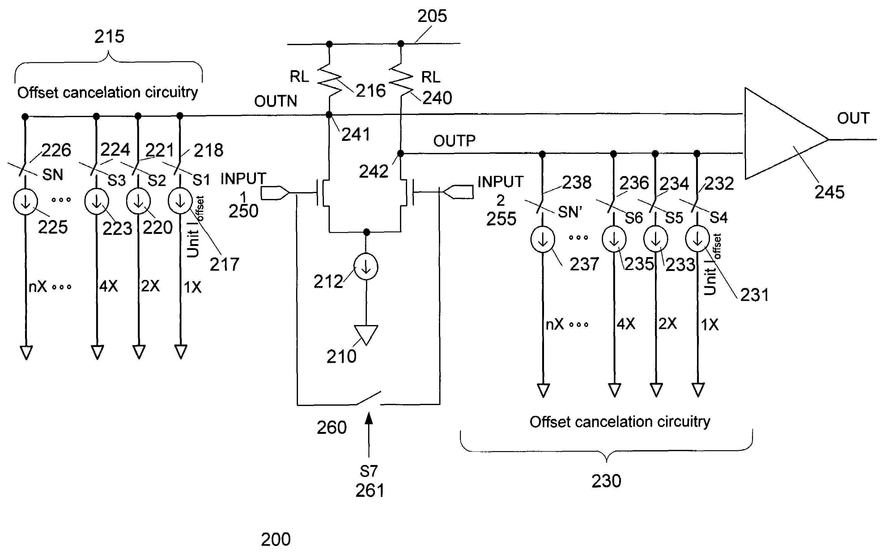
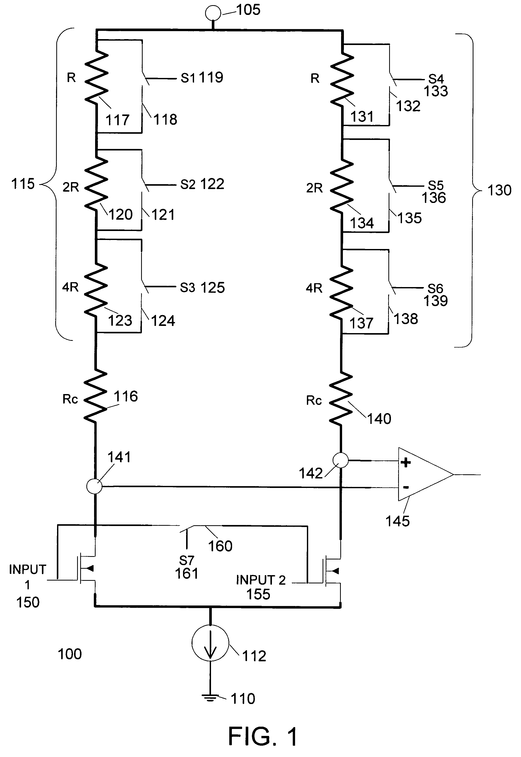
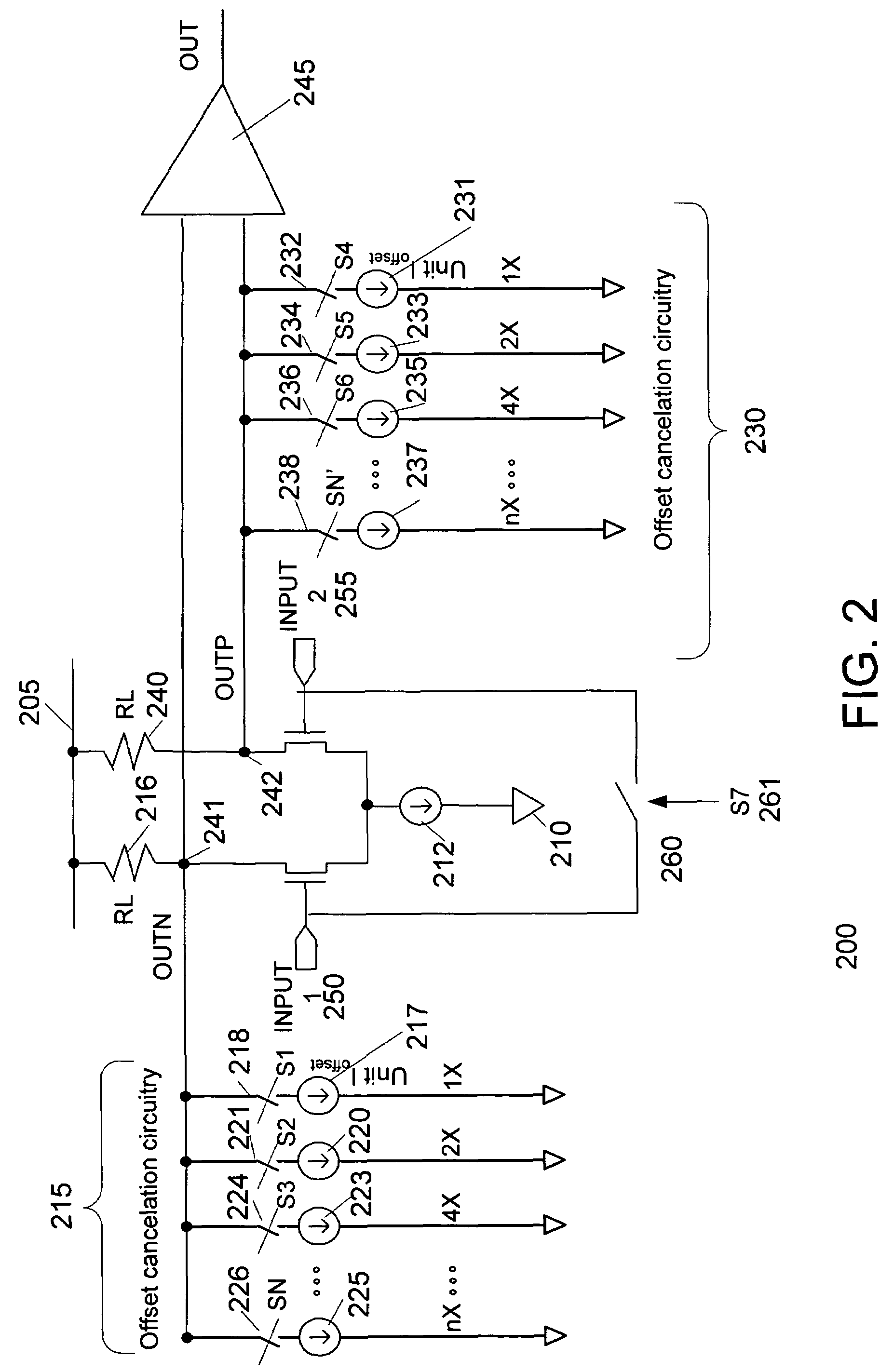
[0018]FIG. 1 illustrates an impedance compensation circuit 100 according to an embodiment of the invention. Impedance compensation circuit 100 is connected with a voltage supply 105 and a ground 110. Current source 112 provides a bias current. Impedance compensation circuit 100 includes first and second inputs 150 and 155 connected with an amplifier or comparator 145. Inputs 150 and 155 are connected with voltage supply 105 via their respective pull-up resistors 116 and 140. Programmable impedance circuit 115 is connected between pull-up resistor 116 and voltage supply 105. In an embodiment, programmable impedance circuit 115 includes a set of resistors, such as resistors 117, 120, and 123. In an embodiment, resistor 120 has a resistance of twice the resistance of resistor 117. Additionally, resistor 123 has a resistance of four times the resistance of resistor 117.

[0019]Each resistor of programmable impedance circuit 115 is paired with a bypass switch controlled by a switch input s...


PUM


Abstract

An impedance compensation circuit for inputs of a programmable device includes programmable impedance circuits connected with input nodes. The programmable impedance circuits can be configured to apply a compensating voltages to input nodes to reduce or eliminate unwanted offset voltages. An impedance compensation circuit may include resistors in series or current sources in parallel. A set of bypass switches selectively apply each resistor or current source to an input node, thereby changing the offset voltage of the node and compensating for impedance mismatches. Control logic provides signals to control the bypass switches. The control logic may be implemented using programmable device resources, enabling the control logic to be updated and improved after the manufacturing of the device is complete. The control logic can automatically evaluate offset voltages at any time and change compensating impedances accordingly. This reduces manufacturing costs and takes into account temperature and aging effects.

Description

CROSS-REFERENCES TO RELATED APPLICATIONS[0001]This application is related to U.S. patent application Ser. No. 11 / 245,581, filed Oct. 6, 2005, and entitled “Programmable Logic Enabled Dynamic Offset Cancellation” and U.S. patent application Ser. No. 11 / 323,372, filed Dec. 29, 2005, and entitled “Signal Offset Cancellation,” both of which are incorporated by reference herein for all purposes.BACKGROUND OF THE INVENTION[0002]The present invention relates to the field of programmable devices, and the systems and methods for detecting and compensating for unwanted offset voltages in the same. Programmable devices, such as FPGAs, typically includes thousands of programmable logic cells that use combinations of logic gates and / or look-up tables to perform a logic operation. Programmable devices also include a number of functional blocks having specialized logic devices adapted to specific logic operations, such as adders, multiply and accumulate circuits, phase-locked loops, and memory. Th...

Claims


Application Information

Patent Timeline
Patent Type & Authority Patents(United States)
IPC IPC(8): H03L5/00
CPCH03F3/45183H03F3/45632H03F2203/45212H03F2203/45646H03F2203/45681H03F2203/45702H03F2203/45726
Inventor WONG, WILSONLAI, TIN H.SHUMARAYEV, SERGEYPATEL, RAKESH H.
Owner ALTERA CORP
Why Eureka
Try Eureka