Total internal reflection micro lens array

a micro-lens array and internal reflection technology, applied in the field of optical devices, can solve the problems of limited angle of divergence of output beam, insufficient angle of divergence, and inability to gain angles

Inactive Publication Date: 2009-06-16
SAMSUNG ELECTRONICS CO LTD
View PDF8 Cites 14 Cited by
  • Summary
  • Abstract
  • Description
  • Claims
  • Application Information

AI Technical Summary

Benefits of technology

[0010]The claimed invention is aimed at developing a device which would allow to widen the angle of divergence of a beam outgoing from a micro structured optics of at least 100 degrees (depending on the used light source), with the efficiency of 80-90% and with totally controllable shape of the outgoing beam.

Problems solved by technology

However there are cases (for example, back light for TFT displays) where such angles of divergence are insufficient and the angle of divergence of radiation must be at least 130 degrees.
This value imposes certain restrictions on the maximum angle of divergence and does not allow gaining angles over 110 to 120 degrees.
The drawback of the said patent consists in limited angle of divergence of the output beam, which is a result of the insufficient refractive index of the used material.
The drawback of the said method consists in difficulty of obtaining uniform light distribution or a specific angle of divergence due to the limited conditions of the incoming radiation or angles of prisms.

Method used


Image

  • Total internal reflection micro lens array
  • Total internal reflection micro lens array
  • Total internal reflection micro lens array

Examples


Embodiment Construction

[0025]The essence of the claimed invention is further explained on the basis of the following drawings.

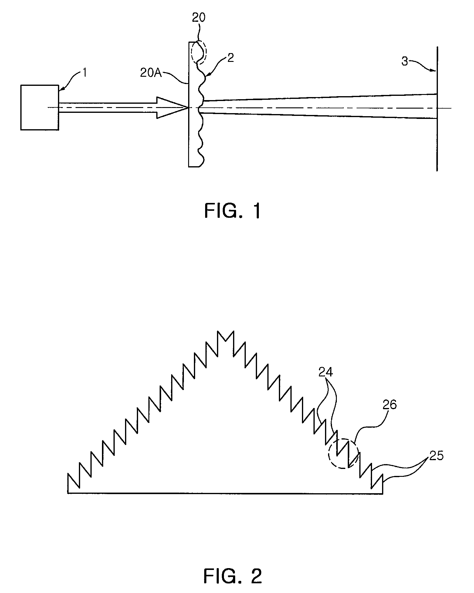
[0026]FIG. 1 shows an optical arrangement including a total internal reflection (TIR) optical microstructure array 2 according to the present invention, where 1 is a light source and 3 is a plane of analysis.

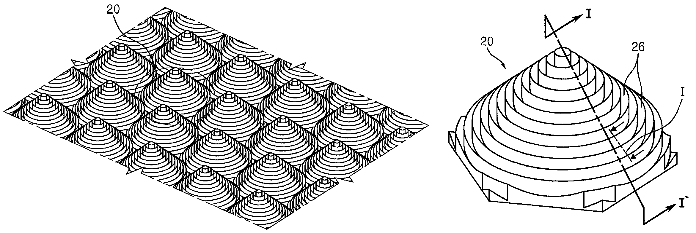
[0027]FIG. 7 is a perspective view of the TIR optical microstructure array 2.

[0028]As shown in FIGS. 2 and 7, the TIR optical microstructure array 2 includes a plurality of optical microstructures 20, which are packed by any known non-periodic or periodic method (for example, the rectangular or hexagonal arrangement). The optical microstructures 20 are arranged on the same optical incidence surface 20A. One optical microstructure 20 of the TIR optical microstructure array 2 is shown in FIG. 8. In this specification, the optical microstructure can be also called a “micro lens”.

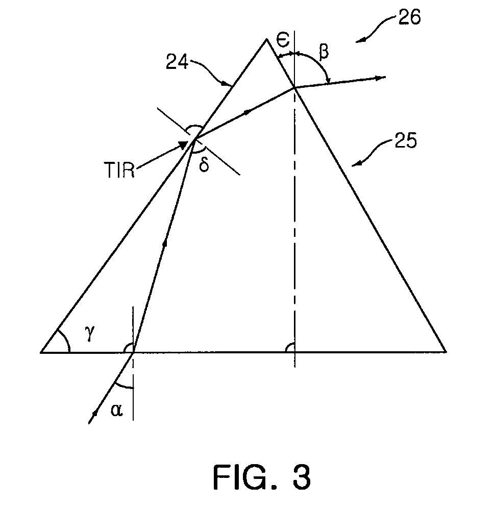
[0029]FIG. 2 is a sectional view of the optical microstructure of FIG. 8 taken along line I-I′.

[0030]Re...


PUM


Abstract

The invention relates to a total internal reflection micro lens array for a wide-angle lighting system. The micro lens array includes a plurality of Fresnel lens structures formed on a same optical incidence surface. Each of the Fresnel lens structure includes a plurality of grooves, each having a reflecting surface and a refractive surface. Incoming radiation incident through the incidence surface of the lens structure is internally totally reflected by the reflecting surface, refracted by the refractive surface and exits the lens structure.

Description

BACKGROUND OF THE INVENTION[0001]1. Field of the Invention[0002]The invention deals with optical devices and can be used in designing the equipment for light beam shaping and spatial restructuring, and more particularly, to a micro lens array designed to make use of the total internal reflection and intended for wide-angle lighting systems.[0003]2. Description of the Related Art[0004]The micro lens array for transformation of light beams is generally used as a structured screen to control propagation (pass) or diffusion of an incident light beam. The micro lens array is a set of micro lenses with sizes from 10 up to 200 micrometers which are packed by one of known methods, for example, by means of the rectangular or hexagonal packing, on one surface.[0005]Existing micro lens arrays enable increasing an angle of divergence of an incident beam up to 110-120 degrees, with efficiency of such devices ranging from 50% to 80%. However there are cases (for example, back light for TFT displa...

Claims


Application Information

Patent Timeline
Patent Type & Authority Patents(United States)
IPC IPC(8): G02B27/10F21V5/00F21V5/02
CPCG02B3/0056G02B3/08G02B17/002G02B17/004G02B17/0856
Inventor KIM, JIN JONGLINKOV, ALEXANDER EVGENIEVICHKIM, HEE DONG
Owner SAMSUNG ELECTRONICS CO LTD
Why Eureka
Try Eureka