Semiconductor device having analog and digital circuits

a technology of semiconductor devices and analog circuits, applied in semiconductor devices, semiconductor/solid-state device details, electrical apparatus, etc., to achieve the effect of reducing the propagation of noise, increasing the clock frequency of the latest semiconductor devices, and increasing the parasitic capacitance of nois

Inactive Publication Date: 2009-06-30
RENESAS ELECTRONICS CORP
View PDF7 Cites 5 Cited by
  • Summary
  • Abstract
  • Description
  • Claims
  • Application Information

AI Technical Summary

Benefits of technology

[0015]An impedance Z of this parasitic capacitance for the noise propagating through a path P shown in FIG. 6 is proportional to 1 / (ωC). Here, the frequency of the noise is ω, and the capacitance value of the parasitic capacitance Cp is C. In other words, the higher the frequency of the noise gets, the easier the noise propagates via the parasitic capacitance caused by the deep well.
[0017]However, the clock frequencies of the latest semiconductor devices have been increased greatly, and as a result, high frequency noises that propagate via parasitic capacitances have come to influence these semiconductor devices.
[0018]The point of the present invention is to reduce the area of a deep well that isolates a well of the opposite conductivity type to a semiconductor substrate from the semiconductor substrate. When a large area is need to be isolated by the deep well, a plurality of deep wells isolated and independent from each other are used and the area of each deep well can be made small.
[0019]By doing the above, the capacitance value of the parasitic capacitance that occurs between the semiconductor substrate and deep well becomes low. Then, the impedance of the parasitic capacitance for a noise becomes high, reducing the propagation of noise.
[0023]According to the present invention, the capacitance value of a parasitic capacitance that occurs between a deep well and a semiconductor substrate can be reduced. Therefore, the impedance of the parasitic capacitance can be made high. As a result, the propagation of noise via the parasitic capacitance can be reduced.

Problems solved by technology

However, since the clock frequency of a conventional semiconductor device was so low that a noise with a frequency high enough to propagate via a parasitic capacitance did not influence the semiconductor device.

Method used


Image

  • Semiconductor device having analog and digital circuits
  • Semiconductor device having analog and digital circuits
  • Semiconductor device having analog and digital circuits

Examples


embodiment 1

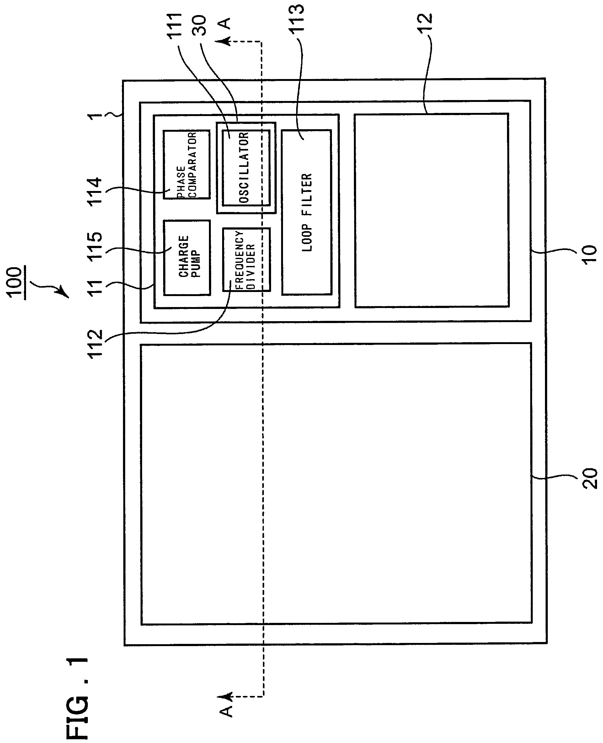
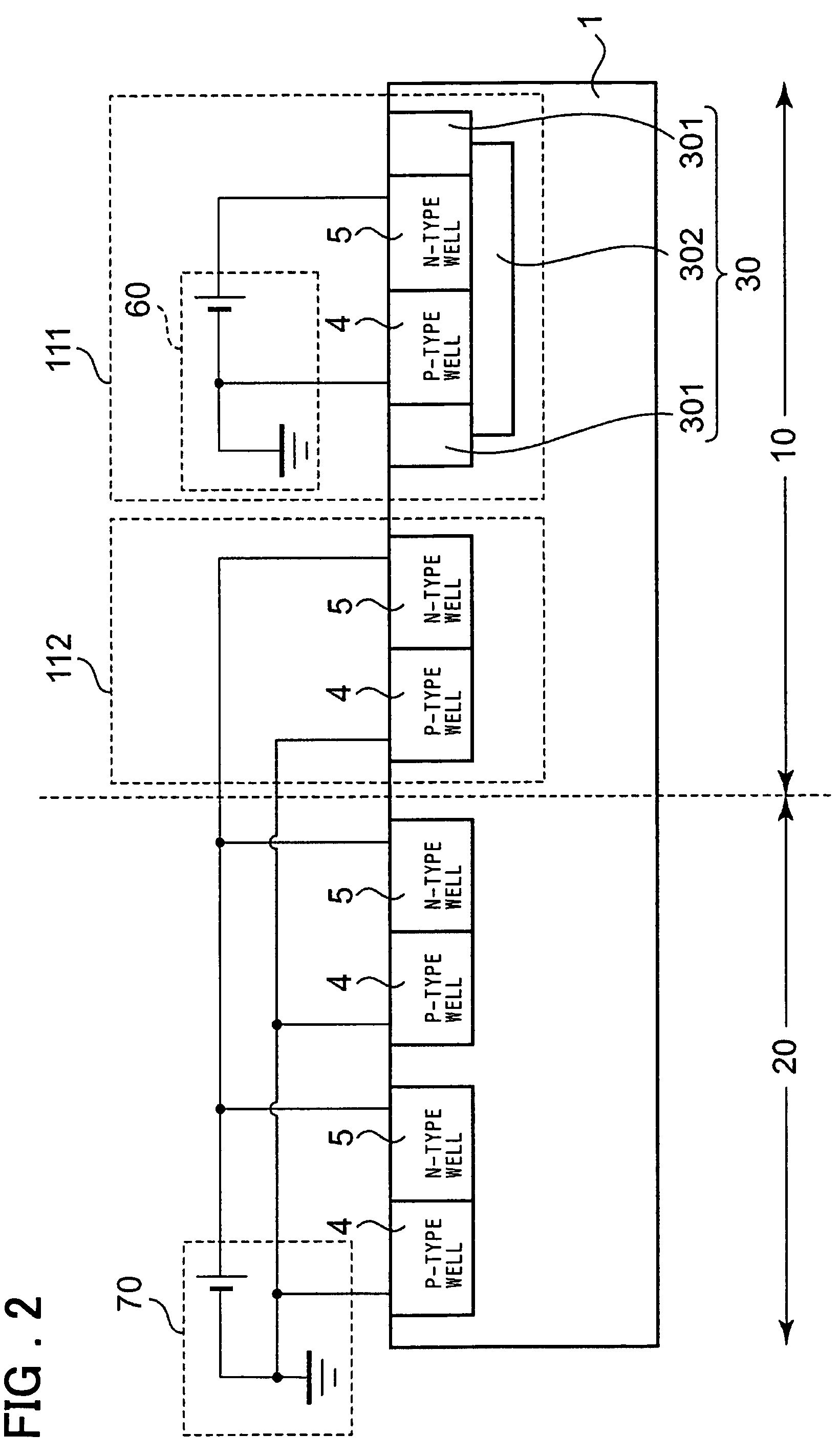
[0030]A first embodiment of the present invention will be described with reference to FIGS. 1 and 2. FIG. 1 is a schematic plan of a semiconductor device 100 relating to the present embodiment. FIG. 2 is a cross sectional view taken along a line A-A in FIG. 1.

[0031]Referring to FIG. 1, the semiconductor device 100 comprises a P-type semiconductor substrate 1, and an analog circuit part (or unit) 10 and a digital circuit part (or unit) 20 formed on the semiconductor substrate 1.

[0032]The analog circuit part 10 includes a PLL circuit 11 and another circuit 12. The PLL circuit 11 comprises an oscillator 111, a frequency-divider 112, a loop filter 113, a phase comparator 114, and a charge pump 115.

[0033]Within the PLL circuit, a circuit constituting the oscillator 111, which is susceptible to noise, is isolated from the P-type semiconductor substrate 1 by an N-type deep well 30. Being “isolated” here means that it is electrically isolated by a depletion layer formed between the N-type d...

embodiment 2

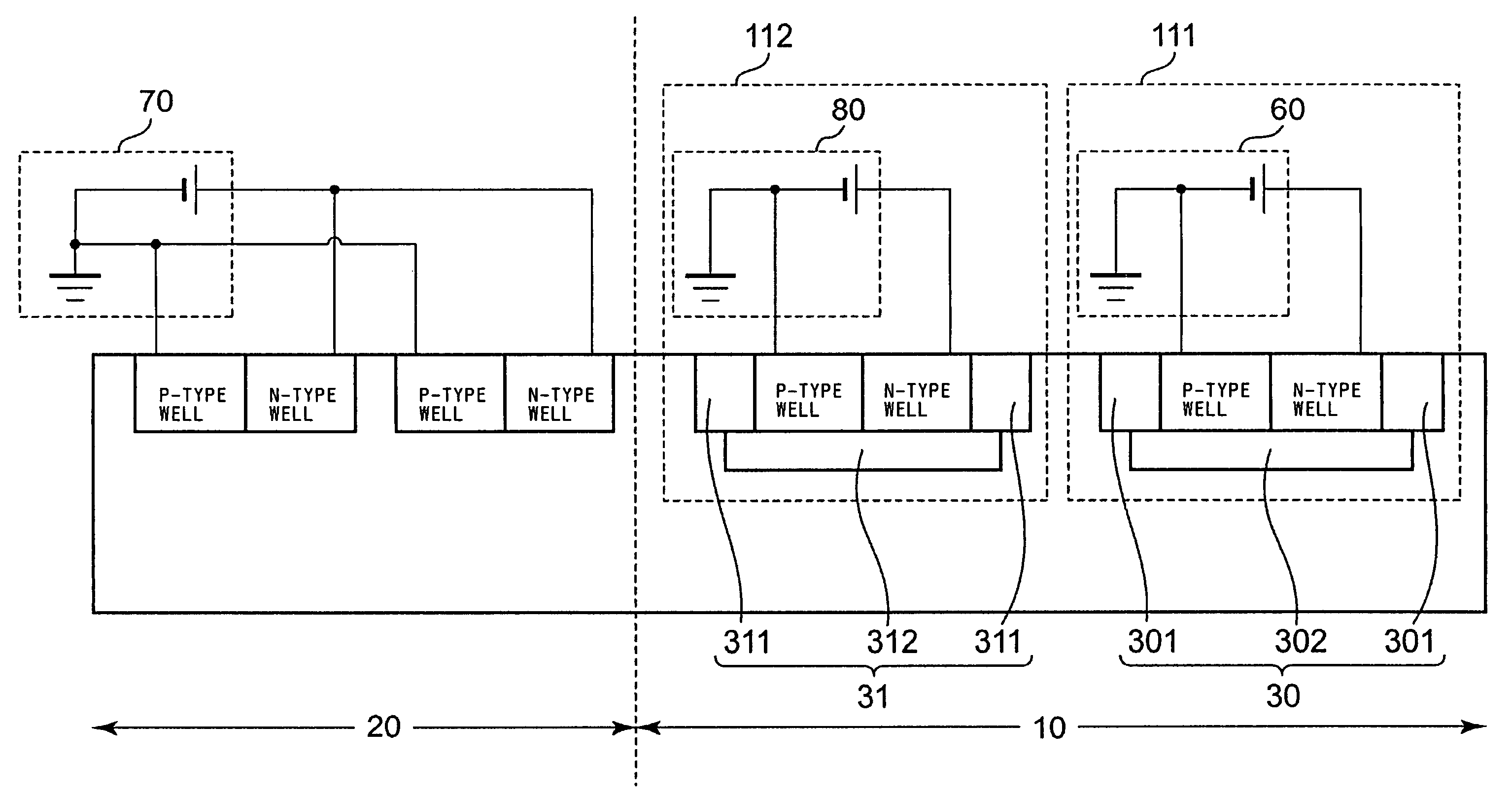
[0039]A second embodiment of the present invention will be described with reference to FIGS. 4 and 5. FIG. 4 is a schematic plan of a semiconductor device 100 relating to the present embodiment. FIG. 5 is a cross sectional view taken along a line B-B in FIG. 4.

[0040]The difference between the present embodiment and the first embodiment resides in that two N-type deep wells (30, 31) are formed and they are isolated and independent from each other. Here, “being isolated and independent” means that a P-type semiconductor substrate 1 or a P-type well (not shown in the drawings) is interposed between the two N-type deep wells 30 and 31, and the potential of one does not essentially influence that of the other.

[0041]In the present embodiment, one of the N-type deep-wells 30 isolates a P-type well 4 constituting an oscillator 111 from the semiconductor substrate 1, and the other N-type deep well 31 isolates a P-type well 4 constituting a frequency divider 112 from the semiconductor substra...


PUM


Abstract

An N-type deep well is used to protect a circuit from a noise. However, a noise with a high frequency propagates through the N-type deep well, and as a result, the circuit that should be protected malfunctions. To reduce the area of the N-type deep well. For instance, in the present invention, a semiconductor device comprises a semiconductor substrate of a first conductivity type, a digital circuit part and an analog circuit part provided on the semiconductor substrate, a plurality of wells of the first conductivity type formed in either the analog circuit part or the digital circuit part, and a first deep well of a second conductivity type, which is the opposite conductivity type to the first conductivity type, isolating some of the plurality of wells from the semiconductor substrate.

Description

FIELD OF THE INVENTION[0001]The present invention relates to a semiconductor device and particularly a semiconductor device having a digital circuit part and an analog circuit part on one substrate.BACKGROUND OF THE INVENTION[0002]In order to reduce the size of a semiconductor device and achieve high functionality, a semiconductor device having a digital circuit and an analog circuit on one semiconductor substrate has been developed.[0003]In such a semiconductor device, there is a problem that a noise that occurs in the digital or analog circuit propagates through the substrate and influences other circuits. Especially, the noise emitted by the digital circuit propagating to the analog circuit through the substrate, and causing the analog circuit to malfunction can be a big problem.[0004]Technologies to solve this problem are disclosed in Patent Documents 1 and 2.[0005]In the technology disclosed in Patent Document 1, a deep well of the opposite conductivity type to a semiconductor ...

Claims


Application Information

Patent Timeline
Patent Type & Authority Patents(United States)
IPC IPC(8): H01L29/76
CPCH01L21/761H01L21/823878H01L21/823892H01L27/0928
Inventor YAMAMOTO, RYOTAKIKUTA, KUNIKO
Owner RENESAS ELECTRONICS CORP
Why Eureka
Try Eureka