Semiconductor device having self-aligned contact and method of fabricating the same

a technology of self-aligning and semiconductor devices, which is applied in the direction of stamping, printing, transistors, etc., can solve the problems of contact failure, patterning process alignment error, and increasing difficulty in forming contact plugs of fine size in desired positions, so as to prevent contact failure

Active Publication Date: 2009-07-21
SAMSUNG ELECTRONICS CO LTD
View PDF9 Cites 18 Cited by
  • Summary
  • Abstract
  • Description
  • Claims
  • Application Information

AI Technical Summary

Benefits of technology

[0013]An embodiment of the invention provides a semiconductor device capable of preventing a contact failure.
[0014]Another embodiment of the invention provides a method of fabricating a semiconductor device capable of preventing a contact failure.

Problems solved by technology

Thus, the aspect ratio of the contact plug increases, and an alignment margin in a patterning process decreases, making it increasingly difficult to form the contact plug having a fine size in a desired position.
However, the patterning process has an alignment error.
As a result, the extended hole 26M causes a contact failure.

Method used


Image

  • Semiconductor device having self-aligned contact and method of fabricating the same
  • Semiconductor device having self-aligned contact and method of fabricating the same
  • Semiconductor device having self-aligned contact and method of fabricating the same

Examples


Embodiment Construction

[0020]The invention will now be described more fully hereinafter with reference to the accompanying drawings, in which exemplary embodiments of the invention are shown. This invention may, however, be embodied in different forms and should not be construed as limited to the exemplary embodiments set forth herein. Rather, these exemplary embodiments are provided so that this disclosure will be thorough and complete, and will fully convey the scope of the invention to those skilled in the art. In the drawings, the thickness of layers and regions are exaggerated for clarity. Like numbers refer to like elements throughout the specification.

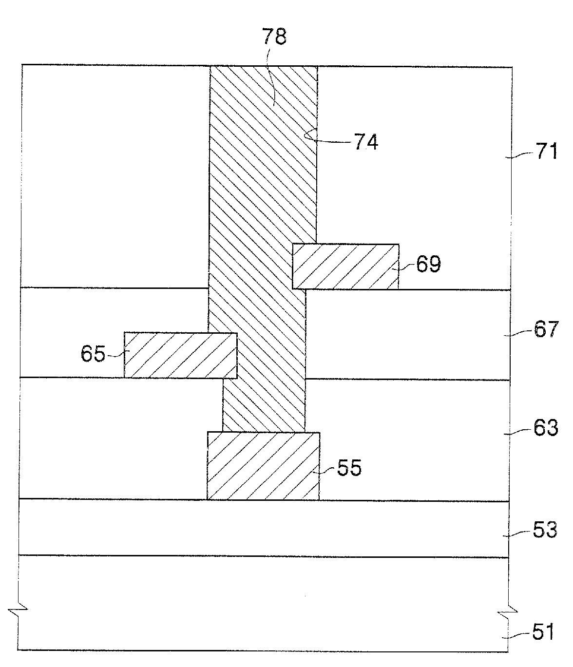
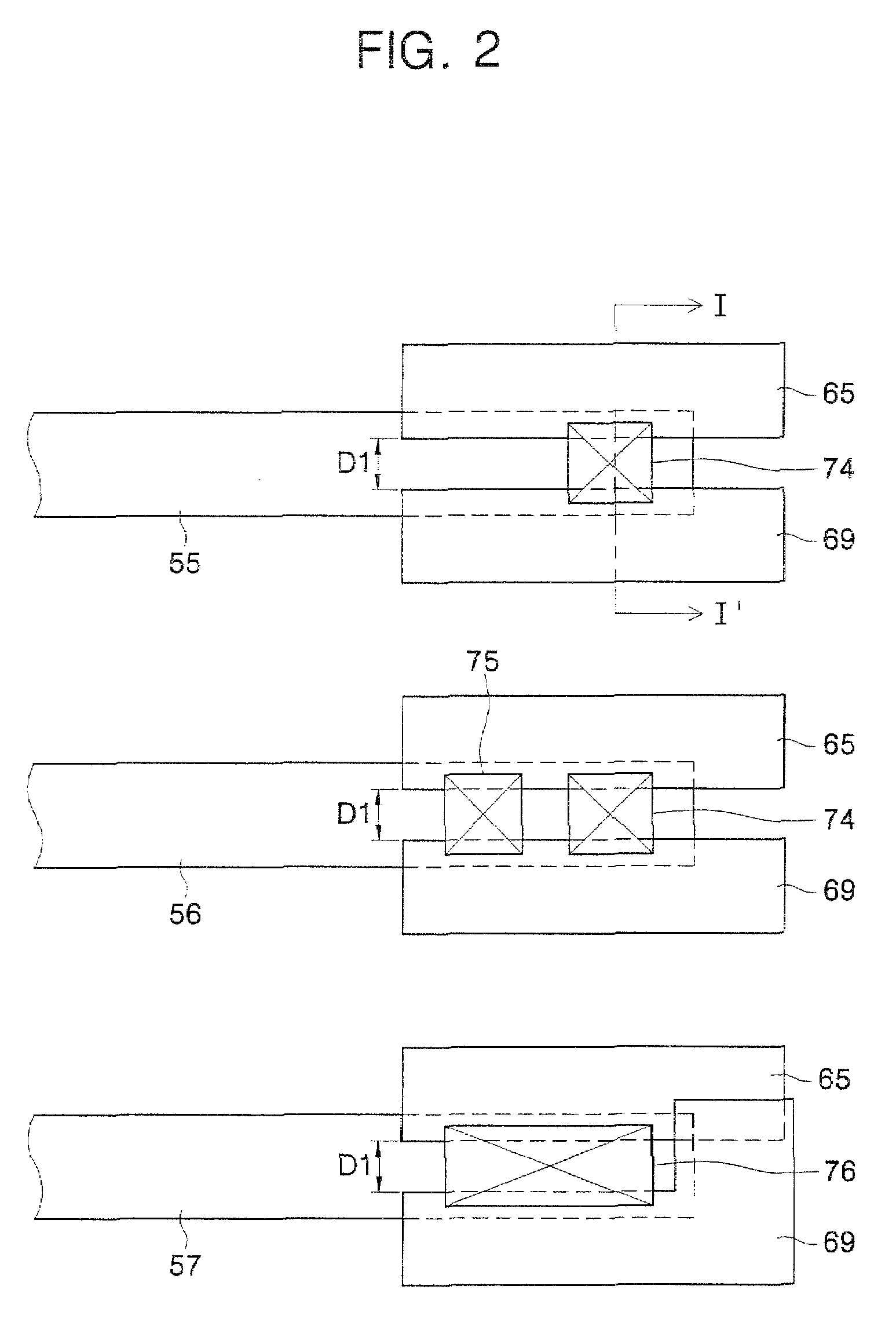
[0021]FIG. 2 is a plan diagram illustrating a portion of a semiconductor device having a self-aligned contact according to some embodiments of the invention, while FIGS. 3 through 8 are cross-sectional diagrams taken along line I-I′ of FIG. 2, illustrating a method of fabricating the semiconductor device of FIG. 2 according to some embodiments of the ...


PUM


Abstract

A semiconductor device includes a conductive pattern disposed on a substrate, a first interlayer dielectric layer disposed on the substrate and the conductive pattern, a first dummy pattern disposed on the first interlayer dielectric layer and partially overlapping the conductive pattern, a second interlayer dielectric layer disposed on the first interlayer dielectric layer and the first dummy pattern, a second dummy pattern disposed on the second interlayer dielectric layer and partially overlapping the conductive pattern, a third interlayer dielectric layer disposed on the second interlayer dielectric layer and the second dummy pattern, and a contact plug that penetrates the third interlayer dielectric layer, the second interlayer dielectric layer, and the first interlayer dielectric layer to contact the conductive pattern, the contact plug arranged between the first dummy pattern and the second dummy pattern, the contact plug abutting the first dummy pattern and the second dummy pattern.

Description

CROSS-REFERENCE TO RELATED APPLICATIONS[0001]This application claims priority from Korean Patent Application No. 10-2006-0006994, which was filed on 23 Jan. 2006. Korean Patent Application No. 10-2006-006994 is incorporated by reference in its entirety.BACKGROUND[0002]1. Technical Field[0003]This disclosure relates to a semiconductor device and a method of fabricating the same, and more particularly, to a semiconductor device having a self-aligned contact and a method of fabricating the same.[0004]2. Description of the Related Art[0005]A semiconductor device, such as a dynamic random access memory (DRAM), may include transistors, capacitors, load resistors, and interconnections. The interconnections include a contact plug that electrically connects conductive patterns. As semiconductor devices become highly integrated, the two-dimensional sizes of components are reduced and a plurality of layers may be required. Thus, the aspect ratio of the contact plug increases, and an alignment ...

Claims


Application Information

Patent Timeline
Patent Type & Authority Patents(United States)
IPC IPC(8): H01L23/528
CPCH01L21/76897H01L28/40H01L27/10888H01L27/10814H10B12/315H10B12/485B41K1/02B41K1/40B41K1/52B41K1/56
Inventor PARK, WON-MO
Owner SAMSUNG ELECTRONICS CO LTD
Why Eureka
Try Eureka